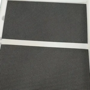
Copper Multilayer PCB
$55.90
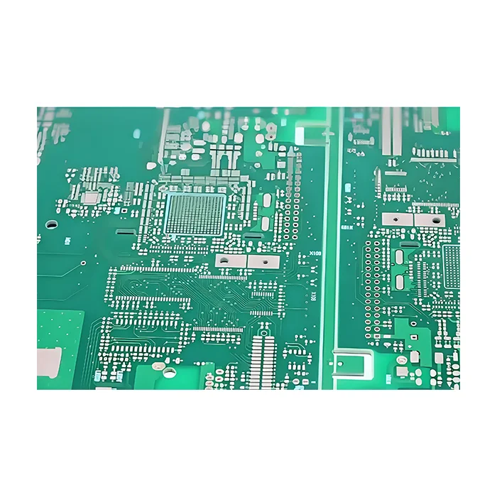
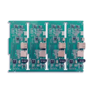
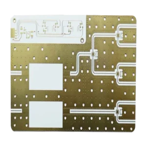
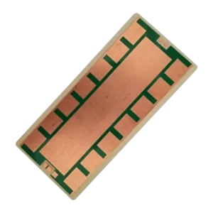
Copper multilayer PCB consists of 3 or more copper conductive layers that are separated by insulating materials. Such PCB is widely used in complex electronic devices that need high-density interconnections, such as smartphones, computers, and medical equipment.
Shipping fee and delivery date to be negotiated. Send inquiry for more details.
Your payment information is processed securely. We do not store credit card details nor have access to your credit card information.
Claim a refund if your order is missing or arrives with product issues, our support team would deal with your refund within 24 hours.
| Layer Counts | 8L |
| Base Material | FR4 |
| Board Thickness(mm) | 1.6mm |
| Max board size(mm) | 570*670mm |
| PCB size tolerance | ±0.2mm |
| Min. Hole Size | 0.15mm |
| Min. Line Width | 4mil |
| Copper Weight | 1oz |
| Surface Finish | ENIG |
| Certificate | UL, RoHS, ISO, ISO9001, ISO13485, IPC610, and REACH |
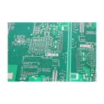 Copper Multilayer PCB
| 5 star | 0% | |
| 4 star | 0% | |
| 3 star | 0% | |
| 2 star | 0% | |
| 1 star | 0% |
Sorry, no reviews match your current selections
Questions & Answers
1. What are your payment terms?
We support T/T, PayPal, Western Union, L/C, and ESROW.
2. Why are multilayer PCBs more expensive than double-sided PCBs?
ENIG is widely used as a surface finish for multilayer PCBs in that it provides sound planarity, solderability, and corrosion resistance. Although it has a higher cost than OSP and HASL, it avoids oxidation issues and supports wire bonding, making it ideal for medical, aerospace, and advanced electronics.
3. Why does impedance control matter in copper multilayer PCBs?
Impedance control in multilayer PCB ensures consistent electrocal properties and maintains signal integrity across high-speed, differential-pair traces, and RF. If there is no careful trace width design to control impedance, the signal is prone to degrade, causing errors and failure in advanced electronics.
4. What causes delamination in copper multilayer PCBs, and how is it prevented?
Delamination in multilayer PCB refers PCB layers separating. It may be because of insufficient lamination pressure, moisture vaporizing, CTE mismatches, and contamination. To prevent delamination, workers will make moisture pre-baking, optimize lamination processes, utilize high-Tg materials, clean the surface, implement thermal management, and more. It depends on practical design and manufacturing.
5. How to design thermal vias in multilayer copper PCBs?
Thermal vias in multilayer copper PCBs are vital for dissipating heat from various components so as to prevent overheating and improve reliability. The key considerations include the via density(50–70% of pad coverage), plating thickness(average 20µm for vias), and the direction of connection with ground and power planes.
6. How does copper thickness affect performance?
Copper thickness impacts PCB’s electrical, thermal, and signal integrity performance. Thicker copper has better current-carrying capacity without overheating and greater heat dissipation, but skin effect can cause signal losses. While thinner copper performs better in signal integrity and is better for fine-pitch components and RF applications, but may increase resistance in power circuits.
7. How many copper layers are common in multilayer PCBs?
The copper layers vary based on different applications, from 2-layer to 20+ layers. 4-6 layers are common in IoT and automotive, and 6-12 layers are widely used in high-frequency designs.
8. What copper foil types are used in multilayer PCBs?
There are 3 main foil types used: Electrodeposited (ED) copper, Rolled Annealed (RA) copper, and Low-Profile copper. From the first one to the third one, they are smoother and pricer. ED copper is cheap but rough; RA copper is smoother for general RF and microwave applications; and Low-profile copper is ultra-smooth for mmWave applications.

