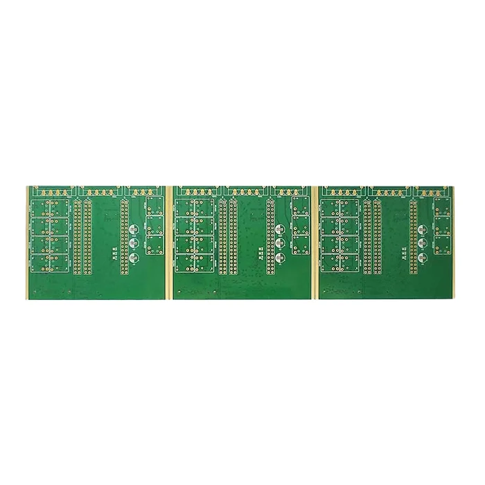
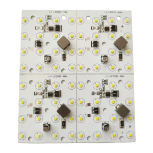
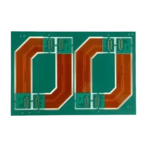
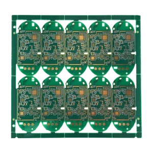
Multilayer PCB Circuit
$38.80
The Multilayer PCB circuit is an electrical board with 2 or more inner layers, and the majority of common multilayer PCBs are usually 4, 6, 8, or 10 layers. Compared to single- and double-layered boards, multilayer PCBs are more dense in circuit arrangement and can include more electrical connections and signal paths, making them prevalent in modern electronic devices, such as consumer electronic appliances like smartphones, telecommunication industries, medical devices, automotive systems, GPS systems, and so on.
Shipping fee and delivery date to be negotiated. Send inquiry for more details.
Your payment information is processed securely. We do not store credit card details nor have access to your credit card information.
Claim a refund if your order is missing or arrives with product issues, our support team would deal with your refund within 24 hours.
| Layer Counts | 4L |
| Base Material | FR4 |
| Board Thickness(mm) | 1.6mm |
| Max board size(mm) | 570*850mm |
| PCB size tolerance | ±0.2mm |
| Min. Hole Size | 0.15mm |
| Min. Line Width | 4mil |
| Copper Weight | 1oz |
| Surface Finish | ENIG |
| Certificate | UL, RoHS, ISO, ISO9001, ISO13485, IPC610, and REACH |
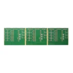 Multilayer PCB Circuit
| 5 star | 0% | |
| 4 star | 0% | |
| 3 star | 0% | |
| 2 star | 0% | |
| 1 star | 0% |
Sorry, no reviews match your current selections
Questions & Answers
1. What is your lead time?
1-2 days. We have our own warehouse and stock in large quantities.
2. Can you mix different copper weights in the multilayer PCB circuit?
Yes. Outer layers(L1/L4) copper weight and inner layer copper can be different, but it requires careful design to avoid compromising structural integrity. What needs to be highlighted is that the asymmetrical distribution can lead to warping caused by uneven thermal expansion. To avoid such a situation, we will add balanced copper or adjust prepreg and core thicknesses to compensate. Common mixing copper can be: thicker copper(2oz or more), for power and ground layers, and thinner copper(5 oz- 1 oz) for signal layers.
3. How many PCB layers can be used for the smartphone? Why should we use so many layers?
Typical smartphone PCBs can use 6-12 layers depending on complexity. Compact smartphones include CPISs, wireless charging, and multiple cameras in a tiny space, which requires high-density interconnects for more connections. More layers enable denser components, better signal integrity, and greater heat dissipation, while keeping the phone thin.
4. What are the key process challenges in multilayer PCB manufacturing?
Key challenges in multilayer PCB manufacturing include 1. precise layer alignment. The multiple layers increase the alignment difficulty; 2. Internal circuit production. A multilayer of lines may cause leakage of the inner layer and influence etching and curling; 3. high-quality via formation. Thick laminate increases the difficulty of roughness and decontamination and may cause drill breakage during drilling. 4. Thermal management. High layer counts are more likely to have resin starvation or Z-axis expansion issues.
5. Why do multilayer PCBs always choose an even number of layers rather than odd layers?
We don’t recommend the odd-layer PCB because they are easier to warping during manufacturing due to uneven copper distribution. On the contrary, the copper of even stack-up PCBs is systematically distributed, which prevents thermal stress and mechanical bending. If you want to customize 3 or other odd PCBs, they need to add extra prepreg or adhesive layer to balance the stack, which makes the circuit more complex and results in a higher cost.
6. Can I reuse a stackup from another project?
Yes. It saves time, but we still need to confirm the material inconsistencies, your design requirements, and manufacturing limitations to ensure the best performance.
7. How does surface roughness (Ra) impact high-frequency PCBs?
Copper roughness impacts signal loss and impedance variations. Rough copper increases resistance and insertion loss, causing skin effect. Rougher copper can also alter effective Dk, leading to impedance deviations.
8. What causes delamination in multilayer PCBs, and how is it prevented?
Moisture absorption and thermal stress are two major reasons. For prevention, workers may preback before assembly, use high-Tg materials, and optimize lamination pressure, control lamination processes.

