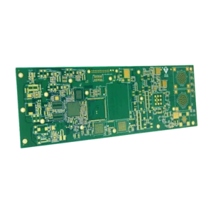
10-Layer HDI Multilayer PCB
$209.90
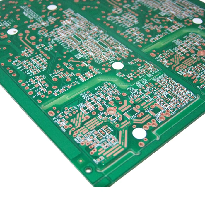
HDI(High-density interconnect) multilayer PCB, typically 6-12 layers or more, is a smaller, lighter, and more compact circuit board with refined line width and spacing, tiny high-precision buried/blind vias, and dense pads. HDI boards deliver higher reliability for compact and high-performance electronic systems, such as telecommunications, automotive, medical devices, consumer electronics, IoT devices, and more.
Shipping fee and delivery date to be negotiated. Send inquiry for more details.
Your payment information is processed securely. We do not store credit card details nor have access to your credit card information.
Claim a refund if your order is missing or arrives with product issues, our support team would deal with your refund within 24 hours.
| Layer Counts | 10L |
| Base Material | Rogers |
| Board Thickness(mm) | 2.0mm |
| Max board size(mm) | 570*670mm |
| PCB size tolerance | ±0.2mm |
| Min. Hole Size | 0.15mm |
| Min. Line Width | 4mil |
| Copper Weight | 2oz |
| Surface Finish | ENIG |
| Certificate | UL, RoHS, ISO, ISO9001, ISO13485, IPC610, and REACH |
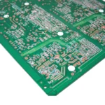 10-Layer HDI Multilayer PCB
| 5 star | 0% | |
| 4 star | 0% | |
| 3 star | 0% | |
| 2 star | 0% | |
| 1 star | 0% |
Sorry, no reviews match your current selections
Questions & Answers
1. What alternate surface finishes are available?
We provide those surface finishes: ENIG, OSP, HSAL, Immersion Silver, ENPIG, and Immersion Tin.
2. What is the optimal aspect ratio in blind and buried via plating?
For blind and buried vias, the optimal aspect ratio is ≤1:1 for reliable plating, and it had better stay 0.75:1.
3. Do you support stacked microvias, staggered vias, or via-in-pad?
Yes, we support stacked microvias, staggered vias, and via-in-pad. Our laser-drilling, precise lamination ensures high-quality HDI circuit PCBs. Let us know your specific requirements, and we are glad to optimize the solution for your project.
4. What should one particularly pay attention to HDI manufacturing?
Drilling reliable vias is one of the core pain points. Proper laser drilling and plating fill is vital to prevent cracking or voids. What’s more, tight trace, space tolerance, precise layer alignment, and high-performance materials are also fundamental considerations in HDI manufacturing.
5. How do you handle blind/buried via alignment in sequential lamination?
Blind and buried via alignment in sequential lamination needs precise drilling and thermal control to avoid misalignment and via failures. The key steps we carefully deal with include stage-by-stage lamination, precision drilling, registration control, and material control.
6. How do I choose between a mechanical and a laser drill?
For HDI PCB, laser drilling is best for microvias and buried/blind vias because of their smaller hole sizes, tighter tolerances. The mechanical drill is suitable for larger through-holes.

