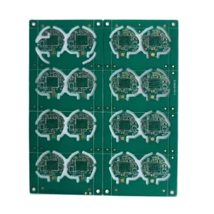
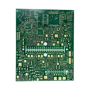
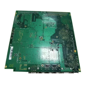
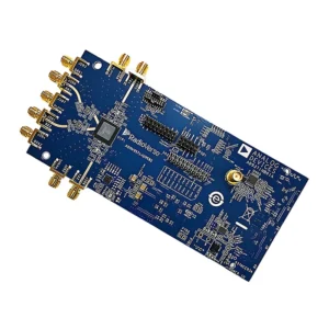
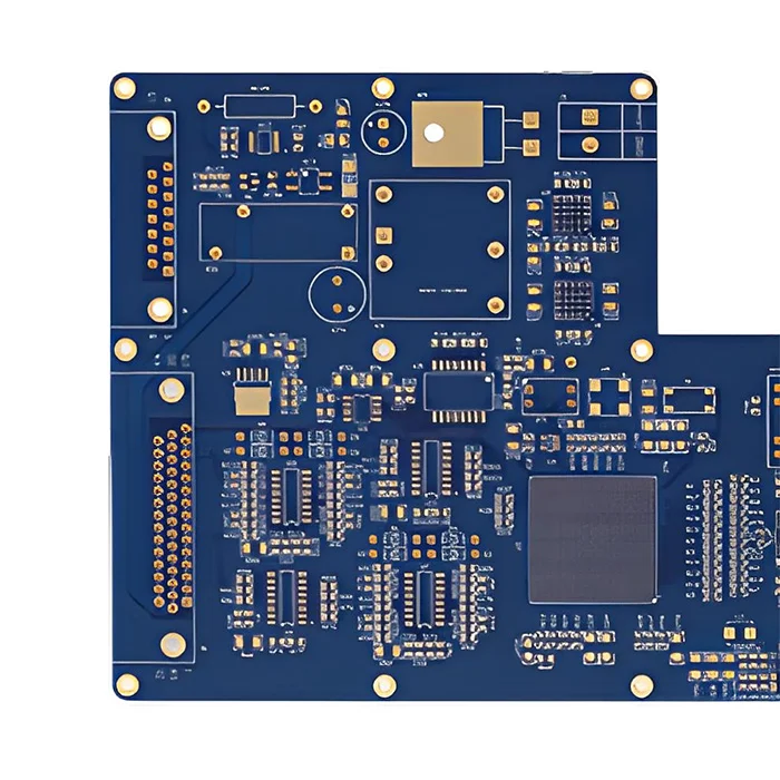
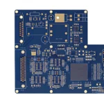
High Frequency PCB 4 Layer
$88.80
This high-frequency PCB is designed with 4 layers of laminations, which are structured for EMI shielding and impedance control. 4-layer High frequency PCB is able to maintain signal integrity and reduce signal loss, which is important for applications that need high-speed signal transmission, RF, and microwave, such as 5G, automotive radar, MRI machines, and so on.
Shipping fee and delivery date to be negotiated. Send inquiry for more details.
Your payment information is processed securely. We do not store credit card details nor have access to your credit card information.
Claim a refund if your order is missing or arrives with product issues, our support team would deal with your refund within 24 hours.
Layer Counts | 4L |
Base Material | Rogers |
Board Thickness(mm) | 1.0mm |
Max board size(mm) | 570*850mm |
PCB size tolerance | ±0.2mm |
Min. Hole Size | 0.15mm |
Min. Line Width | 4mil |
Copper Weight | 1oz |
Surface Finish | ENIG |
Certificate | UL, IPC-6012, RoHS, ISO 9001, ISO14001 |

5 star | 0% | |
4 star | 0% | |
3 star | 0% | |
2 star | 0% | |
1 star | 0% |
Sorry, no reviews match your current selections
Questions & Answers
1. Is international shipping available?
Yes, we ship worldwide and cooperate with DHL, FedEx, and other major logistics companies to deliver medical PCB safely and quickly to you.
2. Why put power planes between signal layers?
The power planes that are put between signal layers can provide shielding to reduce crosstalk, minimize voltage fluctuations, and reduce EMI radiation.
3. How does thermal management affect RF performance?
Excessive heat in RF PCB changes material properties, increases Df, and affects signal integrity. The key influences include the delamination risk for base material that may warp under thermal stress and break solder joints, poor amplifier and oscillators, and shifted resonant frequencies. Designers always use thermal vias, optimized airflow, and metal-core substrates to stabilize performance.
4. 4-layer or 6-layer high frequency PCB, which one should I choose?
Compared to 6 6-layer HF PCB, 4 4-layer HF PCB costs less in manufacturing due to 2 fewer layers. What’s more, if you are looking for low to moderately complex high-frequency circuits, a 4-layer HF PCB is a priority for its cost-efficiency and basic functionality. 6-layer PCB is more complex and justified for applications that require high-speed performance and advanced reliability.
5. Does a 4-layer HF PCB need special vias?
Not necessarily. For standard RF applications(up to ~10 GHz), through-hole vias are sufficient for a 4-layer HF PCB. If the HF PCB is used for mmWave frequencies, it may need microvias to eliminate parasitic stubs that cause signal reflections.
6. How should I route RF signals in a 4-layer HF PCB?
RF signals should be routed carefully to ensure signal integrity, prevent interference, and minimize signal loss. L1 is always used as the layer for RF signals with accurate trace width for controlled impedance and minimal discontinuities. Lay out solid ground planes and power distribution on L2 and L3, and route digital or RF signals on L4.
7. Why do high-frequency laminates overheat faster?
High-frequency laminates like Rogers have lower thermal conductivity. They prioritize low dielectric loss (Df) and stable permittivity (Dk) over thermal dissipation, so designers always need to balance between signal integrity and cooling strategies.
8. Why use back-drilling or buried vias in high-frequency PCBs?
Back drilling and buried vias can minimize signal reflections and enhance bandwidth for high-frequency applications. The unused stubs can lead to signal losses, but backdrilling removes stub portions, and buried vias eliminate them completely.