What Is PCB Routing? PCB routing, the backbone of modern PCB design, is the process of creating PCB trace layout in order to build electronic connections among PCB components. These tiny and convoluted traces are designed digitally with PCB routing software based on routing techniques, and they are curved physically through various fabrication methods, such as using PCB routing machine to cut and mill boards. In this blog, we will lead you to figure out the basic PCB routing secrets about design software and the route fabrication methods, helping route your PCB from the design to reality.
Design PCB Trace with PCB Routing Software
The modern PCB routing combines manual Routing and auto-routing to improve efficiency and quality. Traditional manual routing requires designers to define trace properties and place each trace on the PCB by hand. This offers high control over trace placement, making it crucial for high-speed designs and custom circuits. PCB auto-routing can automatically generate trace paths according to the design rules you set. This may be invaluable for complex and large board design, but it is very effective for dealing with repetitive or basic circuits. Many designers use a hybrid approach: start with auto-routing for basic trace design and manual routing for critical signal paths.
Free & Paid PCB Design Software with Auto-Routing
| Software | Free / Paid | Auto-Routing Support | Best For | Key Features |
| KiCad | Free | ✔ | Beginners & hobbyists | Open-source, strong community support, supports multi-layer PCBs, 3D viewer |
| EasyEDA | Free | ✔ | Beginners & web users | Cloud-based, no installation, integrates with PCB manufacturers |
| DesignSpark PCB | Free | ✔ | Beginners & casual users | Easy to use, large component library, schematic + PCB tools |
| DipTrace | Paid (free trial) | ✔ | Intermediate users | User-friendly interface, 3D preview, supports complex designs |
| Autodesk Eagle | Paid (subscription) | ✔ | General designers & makers | Widely used, integrates with Fusion 360, supports large designs |
| Altium Designer | Paid (high cost) | ✔ (Advanced) | Professionals & advanced users | Powerful manual & auto-routing (Altium auto routing), high-speed design features |
| OrCAD PCB Designer | Paid | ✔ (Advanced) | Professionals & Advanced users | Industry-standard, advanced routing & simulation |
For PCB routing beginners or hobbyists, we recommend you use these free PCB routing software that are easy to operate and save cost, such as Kidcad, EasyEDA, and DesignSpark PCB. EasyEDA is best for those simple and quick projects, in that it is a web-based platform without the need for heavy installation. KiCad is a good tool to learn professional workflow for free because KiCad is advanced with features like 3D viewer and multi-layer PCB support.
For intermediate designers who have the basis of PCB design, we recommend Autodesk Eagle and DipTrace, which are not difficult to master and offer professional-level design and capabilities. Autodesk Eagle provides professional-grade capabilities and strong community support with other Autodesk products without too high cost like Altium. DipTrace is powerful with a clean and user-friendly interface, helping improve your routing skills.
For advanced and professional users, Altium and OrCAD are the best choices. As popular PCB routing tools, they are suitable for professional engineers to solve large-scale or high-density projects, ensuring both performance and manufacturability in complex PCB designs.
How to Route PCB? 6 Basic PCB Routing Techniques
After placing components on the board, we start to route the PCB to build electrical connections. Multiple design tips need to be paid attention to when sizing and routing traces, and the next is 6 basic but important techniques that help avoid issues in the manufacturing process, especially for beginners and hobbyists.
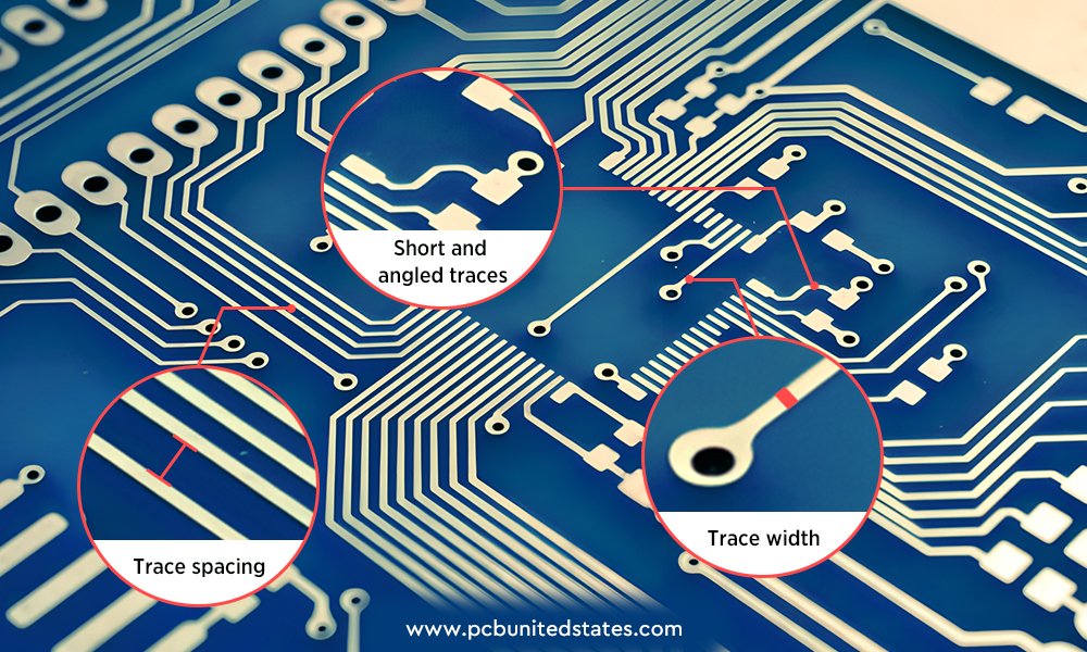
- Appropriate trace width
Size the practical trace width with the trace width calculator according to the current. Thin traces may cause overheating because they can’t withstand too much current passing through. Common signal traces are usually sized about 6-10mil, and power traces are wider about 20+ mil according to the current.
- Keep enough trace spacing
Too close trace distance is prone to risk of short circuits or electrical arcing, especially under high voltage. Generally, low-voltage boards keep 6-8mil spacing, and higher voltage boards increase spacing according to voltage level to ensure safety.
- Keep traces short and direct
Long traces can increase resistance, slow down signals, and pick up noise just like antennas. Besides, bending traces can also cause signal reflection and make trace etching less accurate. Place components beside each other to minimize trace length and use 45°angles for angles rather than 90°right angles.
- Select the ground layer
A ground plane enhances signal stability and helps prevent unwanted noise. On 2-layer board, choose one side to ground; on 4-layer board, reserve 1 entire inner layer for ground.
- Don’t rely on the auto-router
Auto-routers can automatically connect components on the board, but they don’t consider signal integrity, EMI, and thermal dissipation. Just use auto-routing for basic and simple connections and manually route power, ground, and high-speed signals.
- Place vias wisely
Vias connect trace between layers and dissipate heat(thermal vias), but they can also increase resistance and inductance, which can affect high-speed signals. Place Vias only when necessary and keep signals on one layer if possible.
How to Fabricate PCB Routes Physically from Design to Reality?
| Method | Machine / Tools | How It Works | Best For |
| Photolithography + Etching | UV exposure unit, photo plotter, chemical etching machine | Photoresist + UV mask defines traces; chemicals etch away unwanted copper | Mass production |
| PCB Milling (CNC Router Machine) | PCB router machine with fine milling bits | CNC removes unwanted copper mechanically | Prototyping, small batches |
| Laser Direct Imaging | Laser imaging machine, etching system | Directly writes trace patterns on photoresist, then etching | Advanced and high-density PCBs |
| Additive Printing (Inkjet / 3D Printing) | Inkjet PCB printer or 3D printer with conductive ink | Conductive ink printed directly on substrate | Experimental, flexible PCBs, R&D |
PCB milling with PCB Routing machine
PCB routing machine, a type of CNC, is used to route board outlines, mill traces, drill vias, and engrave. CNC routers use fine milling bits to remove unwanted copper and board materials to form traces and create internal features.
This routing method is more convenient for prototype and small batch PCB manufacturing. If you’d like to make PCBs at home, the PCB router machine is a good practice.
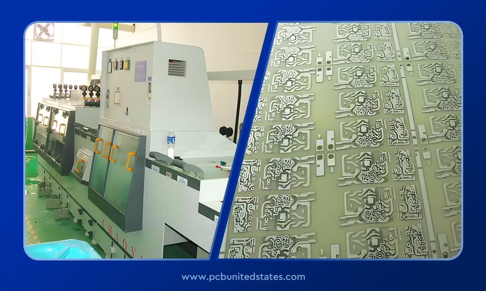
PCB photolithography and etching
PCB etching dissolves unwanted copper by putting the board in the etching solution. The needed circuit traces, pads, and holes are protected by a layer of protective coating on the board that is exposed to UV light, and unprotected patterns are washed away with acid. This is very precise and is useful to make dense and fine traces, standard for industry PCB manufacturing for mass production. MOKOPCB specializes in high-quality PCB fabrication with PCB photolithography and etching. Our factory equipment ensures complex and high-density boards to meet strict quality standards for both prototyping and mass production.
PCB Laser Routing
Laser routing in PCB manufacturing uses high-energy laser beam to directly remove unwanted copper from the board. It excels in creating intricate trace layouts with high accuracy, and the non-contact routing also reduces the mechanical stress, making it ideal for advanced and high-end PCB production.
PCB Printing with 3D Printer
PCB trace printing, by using 3D printing or Inkjet PCB printer, deposits conductive metal ink directly on the substrate to form traces. It is quicker and cleaner without the need of carving or chemicals, though conductivity isn’t as good as copper, so it is always used for experimental designs or flexible PCBs.
Conclusion
PCB routing is the bridge between digital design and working circuit board. For designing your perfect PCB layout, choose the right design software based on your level and needs, such as beginners can choose KiCad or EasyEDA, and apply key routing techniques like proper trace width when sizing and routing traces to ensure the board performs reliably. To make the PCB design become a reality, you can choose different fabrication methods, such as PCB router machine for prototyping and home-made PCB or industry-standard photolithography and etching. Mastering both the software and the manufacturing techniques of PCB routing is key to producing efficient and dependable electronic designs.
MOKOPCB is professional in fabricating high-precision printed circuit boards using advanced technologies, delivering superior quality and reliability for your projects from prototypes. Welcome to contact us if you need professional PCB manufacturing. We are always here to help you bring your design to life.
