Blind and Buried Vias
Blind and buried vias are critical components of high-density interconnect (HDI) circuit technology, which enables more layer-to-layer connections to be made without excessive use of surface or internal routing space. Compared to the traditional through-hole vias, such vias provide more flexibility in stack-up configuration of multilayer PCB, and enable denser routing, since they are placed between particular layers instead of spanning the entire board.
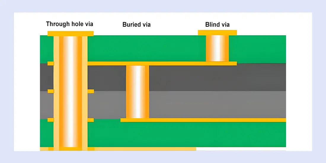
What Are Blind Vias?
Blind vias connect an outer layer of a PCB to one or more inner layers, and do not extend to the opposite side of the board. Depending on its design, they may connect a top layer to an internal layer or bottom layer to internal layer. Once laminated, one end of the via cannot be seen and that is why it is called blind.
What Are Buries Vias?
Buried vias make internal connections between two or more internal layers, but do not extend to the outside surfaces. This kind of via supports greater routing complexity and larger circuit complexity in multi-layer PCB designs.
Key Differences Between Blind and Buried Vias
| Feature | Blind Vias | Buried Vias |
|---|---|---|
| Connection Type | Outer layer to inner layer(s) | Inner layer to inner layer(s) only |
| Surface Visibility | Visible on one surface | Not visible on either surface |
| Testing Access | Accessible from one side | No direct access for testing |
| Routing Flexibility | Frees up opposite surface | Maximizes both outer surfaces |
Benefits of Blind and Buried Vias:
Increased density: Blind and buried vias enable higher component density, and more effective utilization of the board space, as they eliminate unnecessary hole penetrations, and thus creating smaller and lighter PCBs.
Fewer PCB Layers Needed: Selective layer connections enable more efficient routing paths, potentially reducing the total number of layers required in the PCB design, which directly translates to lower manufacturing costs.
Superior Signal Integrity: Both via types reduce electromagnetic interference and crosstalk between traces, thus providing signal integrity and reliability within the system.
Disadvantages of Blind and Buried Vias:
Manufacturing Complexity and Cost: Blind and buried via need special drilling and plating process, which would increase the cost and complexity of the PCB fabrication as compared to typical through-hole via. Also, the fabrication of these vias demand advanced equipment and skills to produce sequential lamination and control the depth precisely.
Limited Testability and Repairability: The presence of buried vias poses particular challenges as there is no surface access point, thus making electrical testing, troubleshooting and repair even more difficult. Blind vias also are only partly accessible, which makes maintenance more complicated.
How to Create Blind and Buried Vias?
Blind and buried vias can be fabricated before or after multilayer lamination process. The production involves drilling of individual core layers and then plating of the holes drilled. Next, the complete layer stack is assembled and laminated together under pressure. The detailed manufacturing specifications can be found in IPC-2221B standards documentation.
When using blind via hole in PCB designs, drill depth control is important. Poor management of depth can have serious impact on boards performance. Too much drilling depth can cause signal integrity problems such as distortion and loss of signal, while insufficient depth can cause unreliable electrical interconnections between layers.
It is necessary to make an efficient collaboration with your PCB fabricator early in the design process to help eliminate the expensive manufacturing difficulty. Be sure that your fabricator also fills the vias with either metal, or thermally / electrically conductive epoxy compounds and copper plates over the filled vias. Inadequate via filling may cause internal air bubbles to work their way up and result in voids, pinholes in the solder joint, etc.
Key Considerations for Blind and Buried Vias
The use of blind vias and buried vias in PCB fabrication and assembly should carefully consider design rules and the manufacturing reliability. The considerations should be the following:
- Vias must cross an even number of copper layers.
- Do not insert vias terminating on top or start on the bottom of a core.
- Blind or buried vias should not overlap(except one is fully enclosed within the other), as that increases the cost since it requires additional lamination/imaging cycles.
- Make sure that there is appropriate plating in viasand have them checked by X-ray.
- Limit the control bonding processes to reduce the delamination riskfrom sequential laminations.
- Fill vias to improve assembly yield and mechanical reliability.
- Assess thermal stress at via locations, especially in the high-reliability applications.
- Use advanced inspection techniques (e.g., microsectioning, thermography) to verify internal via quality.
- Duringdesign planning, consider the limited reworkability of buried connections.
MOKOPCB’s Expertise in Blind and Buried Vias
With extensive experience in advanced PCB fabrication, MOKOPCB is capable of producing precision boards with blind and buried vias. Our engineering team is highly knowledgeable in HDI technologies and can customize via structures to meet the most complex requirements. No matter whether you are in the business of creating smaller consumer electronics or heavy-duty industrial equipment, we can provide you with reliable solutions that fit your project requirements. The table below shows the standard design specifications for blind and buried vias manufactured at MOKOPCB:
| Via Type | Manufacturing Method | Via Diameter (Max) | Via Diameter (Min) | Annular Ring | Min. Copper Thickness |
|---|---|---|---|---|---|
| Blind via | Laser | 0.4 mm | 100 μm | 150 μm | 20 μm |
| Blind via | Mechanical | 0.4 mm | 150 μm | 127 μm | 20 μm |
| Buried via | Laser | 0.4 mm | 100 μm | 150 μm | 20 μm |
| Buried via | Mechanical | 0.4 mm | 100 μm | 150 μm | 20 μm |
For more information or to get a personalized quote, fill in the form and we will get back to you within 24 hours.
Contact Us
Got any questions or inquiries? Fill out the form and we will get back to you soon