Bare PCBs, also named blank PCBs, do not have any electronic components already populated on them. When coming to mass production, bare circuit boards should undergo testing to ensure their reliability and performance. This process, known as bare board testing, focuses on verifying electrical connectivity and detecting defects. By performing tests in the early stage, PCB manufacturers can avoid costly failures later in the assembly process.
What Is Bare Board Testing?
Simply put, bare board testing is performed to ensure that the bare PCB boards have been manufactured correctly and are free of any defects before assembly. During this process, PCB manufacturers usually check:
- Electrical continuity– Check all designed electrical connections on bare PCBs (such as pads, vias, and traces) are properly connected.
- Isolation– Ensure that there are no connections between different circuits that should be designed to remain electrically independent.
- Layout accuracy– Confirm that traces, pads, and vias match the PCB layout.
How to Test Bare PCBs?
Before the PCB assembly process begins, it is critical to test bare boards to ensure they are free from defects. So, how to test bare PCBs? Several methods are available, each varying in accuracy, cost, and speed. Below are the top 5 testing methods.
Flying Probe Testing
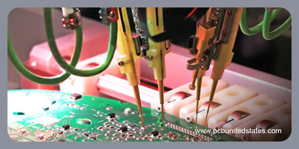
It is an automated test method that utilizes a high-speed probe system. During testing, these probes rapidly move according to a pre-programmed procedure to designated pads, vias, component pins, and other locations, making contact with the circuit board to complete the test. This method can evaluate parameters such as opens and shorts, as well as resistance, capacitance, inductance, and diode polarity.
Pros:
Cost Efficiency in Small Batches: The flying probe test does not need a customized fixture, lowering the initial investment and setup time. A flying probe program can be created and updated within several hours. For small-batch production, it is the perfect solution.
Precise and Reliable Results: This method can provide reliable and accurate testing results, ensuring potential issues are identified before they impact product functionality.
Flexibility for Design Changes: There is no dedicated fixture needed. Flying probe testing adapts easily to different PCB designs and layouts.
Cons:
Slower for High-Volume Production: Compared with ICT, the testing speed of flying probe testing in mass production is slower.
Restricted Component Accessibility: It has limited capabilities to test components with hidden contacts, such as BGAs.
Limited Functional Coverage: This test cannot fully reflect real circuit performance, as it only tests some points. This is only a supplement to functional testing, but not a complete replacement.
In-Circuit Testing (ICT)
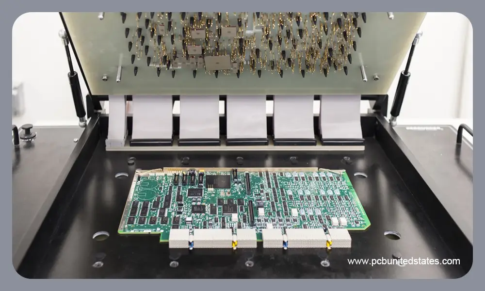
In-circuit testing, also called fixture testing or bed-of-nails testing, is commonly used in large-scale production. This testing method requires a specialized test fixture, integrated with hundreds of probes that accurately contact the testing points. During testing, pressure is applied to the fixture to compress the top and bottom plates, allowing the probes to contact all test points simultaneously. Thus, a comprehensive test of the entire bare PCBs can be completed in a very short time.
Pros:
High Accuracy: With a precise and customized fixture, ICT is a very accurate method for detecting manufacturing faults. This inspection method can quickly and accurately detect component defects, shorts, opens, and other faults.
High Speed: The bed of nails tester can contact all test points at the same time. This method is faster than point-by-point testing, such as flying probe testing. It works well for large-scale manufacturing.
Cons:
Higher Initial Costs: ICT typically requires specialized test fixtures, which must be customized for each bare PCB. ICT machines are also expensive. For small batches of products, the initial investment is too high.
Time-Consuming Program Setup: It takes a lot of time to create ICT test programs, particularly when working with intricate bare PCBs. This can also increase the overall production cycle.
Automated X-Ray Inspection (AXI)
X-ray inspection is an advanced nondestructive testing method that detects defects that are difficult to detect with the naked eye. It works by emitting X-rays through a bare PCB and analyzing the resulting image on a detector. This method can be used to inspect defects in blind or buried vias, misaligned layers, internal traces, connection faults, etc. AXI is typically used to inspect solder joints and component positions during the assembly phase, but is also increasingly being adopted for bare circuit board inspection, particularly for complex or high-reliability PCBs.
Pros:
Non-Destructive: X-rays can penetrate materials and can be used to inspect bare PCBs without damaging them.
Automated & Consistent: AXI minimizes human error by using sophisticated software and algorithms to deliver automated, consistent, and dependable inspection results.
High-Density & Complex Boards: It is essential for inspecting HDI PCBs and components with hidden solder joints, such as BGAs. The X-rays can peer through PCB layers, revealing internal defects that cannot be seen with optical inspection.
Cons:
Require Skilled Operators: Although AXI is an automated inspection, skilled personnel are still required to operate the complex equipment and interpret the detailed X-ray images.
Slower Inspection Speed: Its inspection time is slower and not as fast as AOI, so it’s not well-suited for high-speed production lines.
High Initial Cost: The initial investment, including machine and software costs, is significantly higher than that of other detection methods.
Automated Optical Inspection (AOI)
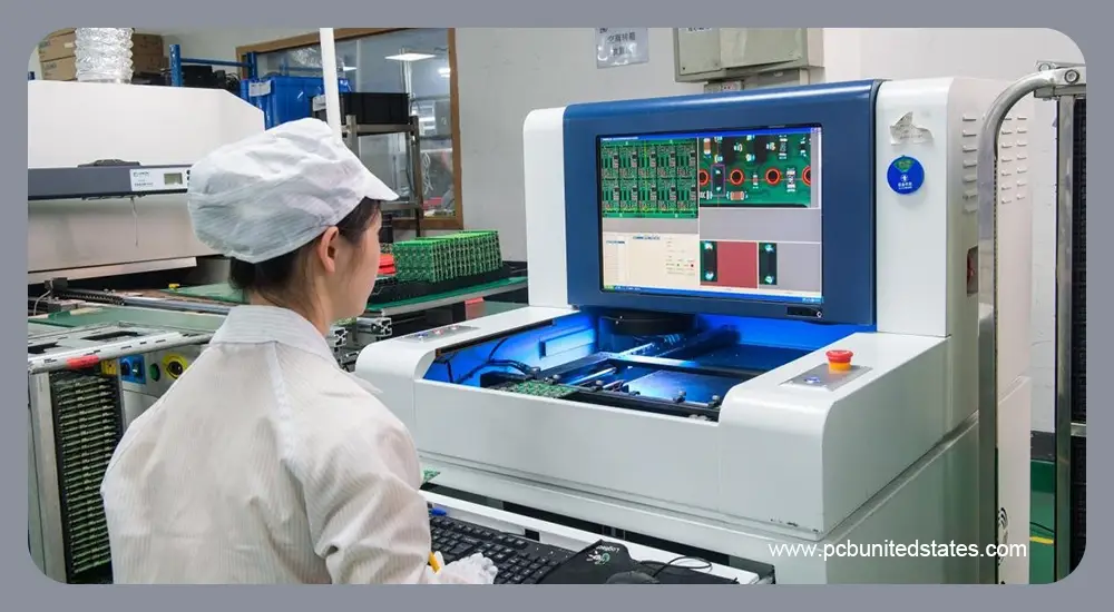
Automated optical inspection takes pictures of the bare PCBs using either two 3D cameras or one 2D camera, then compares the pictures to the schematic. Any discrepancies require manual review. It can detect incorrectly drilled holes, solder mask defects, broken traces, and other issues.
Pros:
Rapid & Non-Destructive: It can test bare PCBs quickly and does not contact or destroy them.
Effective for Surface Defects: This method can accurately detect surface defects on bare PCBs, such as missing components, etching errors, pad defects, etc.
Economical: Compared with AXI, AOI has lower equipment and inspection costs. It works well for regular mass production quality control.
Cons:
Surface-Only Detection: AOI can only detect surface defects and cannot detect hidden solder joints, buried vias, internal traces, etc.
Potential False Calls: It relies on image comparison, which may lead to misjudgment of good bare PCBs or missed defects in some cases, requiring manual review.
No Electrical Testing: AOI doesn’t power the board, so it can’t detect electrical problems like shorts or opens. Therefore, it’s often combined with other testing methods.
Burn-In Testing
Burn-in testing is a destructive test used to detect potential bare PCB failures early and verify their load capacity. It involves subjecting electronic products to prolonged exposure to high temperatures, loads, or other stresses. This process typically lasts 48 to 168 hours, allowing potential defects to become apparent early under these extreme conditions.
Comparison of Bare PCB Testing Methods
| Types | Contact Type | Test Type | Inspection Speed | Cost | Batch Suitability |
| Flying Probe Testing | Contact | Electrical test | Moderate | Moderate cost, no fixture needed | Small batch |
| ICT | Contact | Electrical test | Fast, efficient for mass production | High cost, customized fixture required | Medium to large batch |
| AXI | Non-contact | X-ray inspection | Fast for high-density boards | High cost, expensive equipment | Medium to large batch |
| AOI | Non-contact | Optical inspection | Moderate | Moderate cost, easy setup | Medium to large batch |
| Burn-In Testing | Non-contact | Reliability test | Slow, long test cycles | High cost, energy, and time-consuming | Small to medium batch |
Why Is Bare PCB Testing Important?
While many companies consider bare board testing to be time-consuming and costly, its importance cannot be ignored. It offers three key benefits that make it an essential step before PCB assembly.
Lowering Manufacturing Expenses
A small investment in bare board testing can save significant later repair and rework costs. When manufacturing bare PCBs, some common defects may occur, such as excessive or missing copper, short circuits, and extra holes. Once the board is populated with components, inspection becomes increasingly challenging. Ultimately, if a board fails, expensive components may be wasted, and repair costs also increase.
Improved Assembly Yield
Some errors may be difficult to notice in the early PCB design stages. By testing the bare PCBs during the prototype stage, it’s easy and possible to identify and resolve the potential defects. This can ensure a smoother assembly later on, decreasing the risks of interruptions, delays, and assembly failures.
Enhanced Product Reliability
When conducting bare board testing before assembly, you can ensure these boards perform as expected. Once missing this process, a high rate of subsequent PCB failures can negatively impact your company’s reputation. Reliable bare PCBs also mean fewer returns and claims, leading to greater customer satisfaction and increased product trust.
How to Select the Best Testing Method for Bare PCBs
When choosing the right testing methods, you should consider several factors. Here are five critical factors:
Evaluate Product Requirements
For simple bare PCBs used in consumer electronics, simple and affordable inspection methods are often sufficient. For high-density or high-reliability boards, it’s recommended to invest in more advanced test methods. You can choose a combination of multiple inspection methods, which can ensure reliable test results.
Factor in PCB Layout Complexity
It’s critical to consider the PCB design complexity, which may not match some testing methods. If it is a high-density board with fine traces and multiple layers, advanced testing techniques may be required to ensure reliable test results.
Take Production Quantity into Account
PCB production volume also influences the choice of test method. Flying probe testing is more flexible and cost-effective in small-scale production. For high-volume production, automated methods like bed-of-nails testing offer higher speed and consistent test results.
Account for Cost Limitations
Some test methods, such as bed-of-nails and AXI, require a higher upfront investment. Bed-of-nails fixtures and AXI equipment are expensive and may not be suitable for small-scale production.
Adopt a Hybrid Approach
In some cases, multiple methods can be used to balance cost and reliability. For example, critical areas of bare PCBs can be inspected using AXI, while less critical areas can be inspected using AOI.
Takeaway
Bare board testing is a critical step before the PCB assembly process, ensuring a smooth production cycle. Proper testing is crucial to ensuring the reliability of bare PCBs and avoiding costly issues later on. At MOKOPCB, we understand the importance of quality control and testing, and we utilize state-of-the-art inspection to ensure the highest quality bare boards. If you have any questions, please feel free to contact us, and we’ll discuss the best testing methods for your bare PCBs.
