Plated Half-Holes
The technology of plated half-hole has gained popularity in the design of PCBs because it helps to make interconnection between the boards mechanically and electrically. These half-plated holes provide ease of module-integration and compact assembly without using large-sized connectors.
Along with the increased demand for smaller and more efficient electronic devices, plated half-holes provide an effective method to improve the functionality and manufacturing efficiency of circuit boards. Understanding their benefits, PCB plated half-hole size requirements, and design considerations is essential for modern PCB development.
What Is a Plated Half-Hole in PCB?
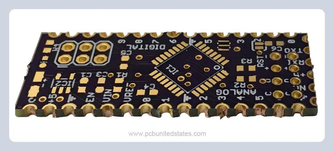
Plated half-holes or castellated holes are holes that are drilled along the edges of a rigid PCB. These holes are plated through and then partially milled to form a half-hole shape. They are typical used in Wi-Fi modules that are soldered directly onto main circuit boards as integrated circuits are. The main use of castellated holes is to facilitate board-to-board connections, especially where two PCBs are connected by using two different technologies.
Advantages of Using Plated Half-Hole
Easy to handle and solder
Plated half-holes can be accessed more quickly during assembly because they are on the edge of the module. As opposed to surface-mount pads on the underside of a module, which can obstruct component placement, edge-mounted half-holes make soldering easy.
Improved alignment
Pads located underneath a module can increase the risk of misalignment during assembly. Connection points on castellated hole designs are located on the edge of the PCB, and this simplifies the alignment of the module to the matching board, hence reducing the chance of alignment mismatch.
Simplified measurements
In a plated half- hole, it is easy to measure the distance between holes and solder joints even after the module has been installed. This measurement can be done with calipers, which is not feasible when pads are located beneath the module.
Cleaner board surfaces
Modules with castellated holes act as surface-mount subassemblies, which means they can be mounted directly onto another PCB just like any other SMD component. Such a close fit reduces areas in which dust or debris may be trapped between the two boards.
How to Design Castellated Holes? 7 Guidelines to Follow
When designing plated half-holes, keep the following guidelines in mind:
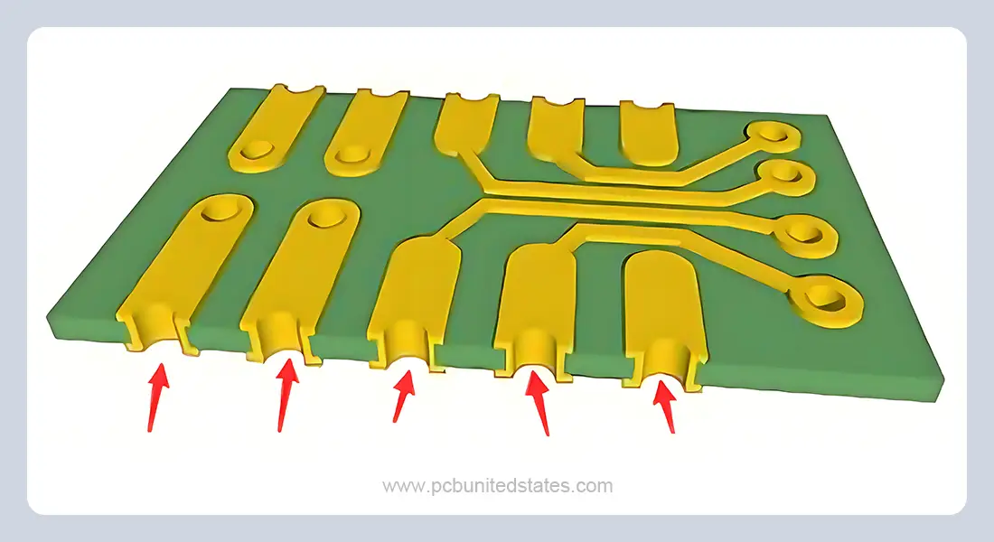
- Locatethe center point of each castellated hole at the exact edge or boundary of the PCB (in case of oval holes, ensure that the start and end points of the hole are accurately placed).
- These holes should be defined as plated through-holes on your EDA software. Note that when you supply Gerber files, you need to supply holes/slots in the drill files (*.drills_pth.xln or *pth.drl files).
- Each castellated hole should be placed within a pad on every copper layer (including inner layers on multi-layer boards) to provide adequate stability for the copper sleeve.
- Make sure the pad completely surrounds the hole. Pad and annular ring requirements should match those of standard through-holes.
- A half-hole should generally have a diameter of no less than 0.6 mm. Plated half-hole size considerations are critical for ensuring reliable connections and manufacturability.
- The minimum distance between the edges of two holes is 0.55 mm. Although it can vary between 0.47 mm and 0.55 mm, it can add to the manufacturing cost and increase production time.
- The solder mask bridge should be at least 0.1 mm wide.
For detailed specifications, see the table below (unit: mm).
| PCB thickness | Plated half-hole limitation | Plated half-hole diameter | Min. size after routing |
|---|---|---|---|
| ≤1.0 | 0.4 | 0.4 | 0.25 |
| 1.2-1.6 | 0.4-0.6 | 0.25 | |
| 0.7-0.9 | 0.35 | ||
| ≥1.0 | 0.45 | ||
| 2 | 0.4-0.6 | 0.25 | |
| 0.7-0.8 | 0.4 | ||
| ≥0.9 | 0.45 |
The Production Process of Plated Half-Holes
Plated half-holes are traditionally produced through multiple processes: drilling, chemical copper deposition, image transfer, pattern plating, film removal, etching, solder mask printing, surface treatment, hole formation, and contour milling. Nevertheless, this traditional method sometimes lowers productivity and product performance.
Today, there are more advanced methods for creating castellated hole. Usually, the process begins by drilling the PCB edge, which necessitates a precise and specialized drilling machine, as errors at this stage will affect all subsequent manufacturing procedures. Copper plating is then applied to the holes after drilling. This is an important step to ensure reliable electrical conductivity of the components mounted on the board.
Applications of Plated Half-Hole
Plated half-holes have many applications in modern PCB design and manufacturing, providing a broad range of solutions for interconnection problems:
Modular PCB Design: Castellated holes facilitate the creation of detachable sub-modules from larger PCB assemblies, making modular system architecture possible.
Flexible Component Integration: These edge connections allow flexible pin arrangements and component layouts to be customized to suit specific design requirements without the need to redesign entire boards.
Module-to-Mainboard Assembly: During surface-mount assembly processes, castellated holes are used in integrated circuit modules to ensure both mechanical and electrical connection with main PCBs.
Board-to-Board Mounting: PCBs with castellated edges can be surface-mounted directly to parent boards and no connector is required.
Compact Module Applications: Widely used in compact design applications like WiFi modules, Bluetooth modules, and other communication devices in small sizes.
Direct PCB Interconnection: Castellated holes allow direct board-to-board electrical connections without using typical wire harnesses or large connectors and are found in compact wireless and communication systems.
MOKOPCB’s Capabilities in Plated Half-Hole PCB Manufacturing
MOKOPCB focuses on manufacturing high-quality PCBs with plated half-holes, both for prototyping and high-volume production. We meticulously optimize every design to improve hole positioning precision, smooth plating, and high solderability. Our state-of-the-art manufacturing facilities deliver consistent quality and rapid turnaround. With vast experience in serving areas like IoT, telecoms, and consumer electronics, we are able to cater to the most stringent customer castellated hole needs.
When you need a trusted company to design and fabricate PCBs with castellated holes, you can count on MOKOPCB. Contact us now to discuss your project and get a fast quote.
Contact Us
Got any questions or inquiries? Fill out the form and we will get back to you soon