Side Plating
Side plating (or, edge plating, or castellation) is a very important PCB manufacturing technique used in RF, microwave, and other challenging applications. It is the process that offers comprehensive solutions to problems of electrical connection, electromagnetic shielding, and mechanical strengthening. Here, you will learn when side plating is required, the advantages of edge plating, and the key design and manufacturing rules.
What Is Side Plating in PCB?
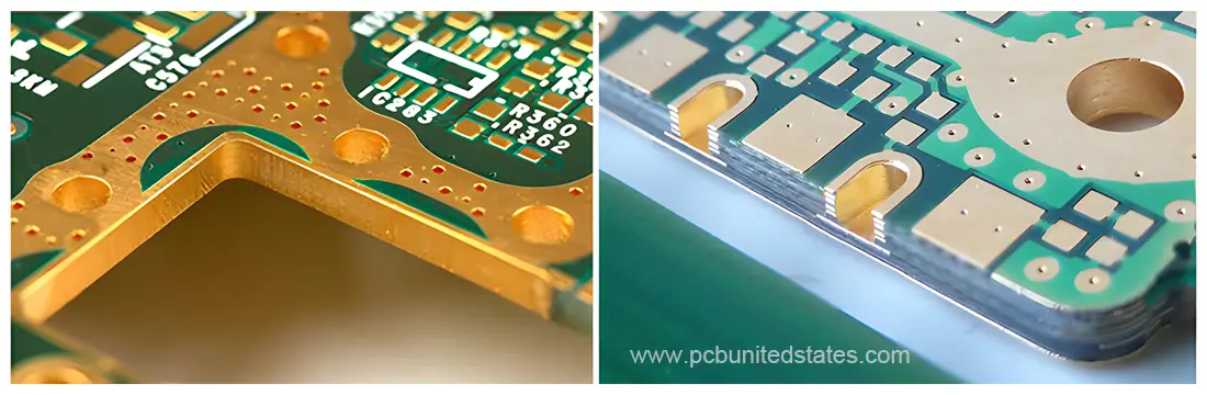
Side plating refers to metallization of edges of a circuit board in PCB manufacturing process. It is basically the application of copper plating that extends from the top of the board to the bottom of the board, continuing along one or more of the external edges of the board. Such a plated surface can be coated with various surface finishes: ENIG, ENEPIG, HASL, other treatments to ensure electrically conductive performance. Side plating allows the PCB edge to serve functional purposes during assembly, and both the board’s outline and certain interior sections can be metalized.
Benefits of PCB Side Plating
Side plating provides several benefits that make it the crucial PCB technology in challenging applications:
Improved Electrical Connectivity
Side plating forms continuous electrical contact among different PCB layers, so it is particularly useful where signal integrity requirements are high. It improves the transmission of high-frequency signals and is frequently used in RF and microwave applications in which signal quality is vital.
Enhanced Electromagnetic Compatibility (EMC)
Side plating can be considered a Faraday cage for the PCB. It helps reduce unwanted electromagnetic noise and keeps delicate internal circuits safe from outside interference. Using this technique, the PCB will be able to satisfy EMC requirements and ensure stable operation even under high electromagnetic interference (EMI) environments.
Strengthened Mechanical Support
Edge metallization offers robust mechanical support for the PCBs, which are more resistant to sideways pressures and mechanical stress. This brings benefits to circuit boards that need to handle frequent use, vibration, and those used in demanding environments.
Better Thermal Management
Side plating offers a backup conductive path that helps improve heat dissipation. This characteristic is particularly advantageous for applications running on high power as it assists in keeping internal temperatures safe and thus prolongs the PCB’s lifespan.
When Edge Plating Is Needed?
Side plating is typically used in PCB manufacturing for both functional and mechanical purposes. It is required in the following situations:
Improved Conductivity – To enhance the overall electrical conductivity of the PCB.
Edge Connections – When electrical connections need to be made directly on the PCB edge.
Mechanical Protection – To strengthen the board edges and prevent damage from lateral impacts.
Board-to-Board Connections – When a secondary PCB connects to the main board through its edge.
How to Design Edge Plating in Your PCB Layout?
For successful side plating manufacturing, designers must use overlapping copper elements—such as copper surfaces, pads, or traces—to mark the metallized regions in their CAD layout files. Key design requirements include:
- The minimum overlap should be 0.5 mm.
- For connection layers, a copper trace of at least 0.3 mm must be established.
- On non-connection layers, copper should maintain a minimum distance of 0.8 mm from the outer edge of the board contour.
Top 7 Design Considerations for Edge Plating
When designing your PCB with edge plating, these are some of the key considerations you must follow to maintain correct functionality and manufacturability:
- Maintain spacing of at least 10 mil between side plating and nearby copper elements. During design phase, it is recommended to check these spacing requirements with your manufacturer.
- To prevent undesirable electromagnetic coupling and possible short-circuit states, ensure non-grounded edge plating is adequately separated from signal routing.
- Drill holes away from the edge of the board. If yourdesign demands plated holes near metallized edges, then you should communicate with your contract manufacturer to ensure the feasibility.
- Ensure that edge plating does not interfere with edge-mounted connectors such as SMA; openings in the plating are required to allow these parts to connect to the board.
- In situations where you have castellated holes on your design, the edge plating is supposed to be extended round them to form the solder pads for attaching to baseboards.
- Any planes that require connection to the side-plated area must extend past the PCB edge.
- Effective grounding and shielding can be ensured by removing solder mask over those areas where edge plating willinterface with shielded enclosures.
Manufacturing Process of Side Plating
Step 1: The PCB edges are first milled, cleaned, degreased, and roughened. This preparation removes contaminants that promote strong adhesion of the plating material, ensuring uniform coverage.
Step 2: To provide a smooth, uniform layer of copper on the overall board, including edges, an electroless copper plating bath is used. This initial coating is conductive in nature and upon it subsequent plating will occur.
Step 3: The board is then subjected to electrolytic copper plating, during which a thicker layer of copper is deposited on the board edges, which improves durability and conductivity.
Step 4: Unneeded copper is removed by chemical etching, and the needed circuit pattern and plated edges are preserved.
Step 5: Edges are micro-etched or otherwise surface-treated to eliminate oxides and enhance the adhesion of successive finishes so that plating is complete and consistent.
Step 6: The plated edges are then given a final surface finishing of a plated finish- like ENIG. This increases solderability, corrosion resistance, and mechanical strength.
Step 7: The boards are cleaned and dried in order to remove any remaining chemicals or debris from the plating procedure.
Step 8: The PCB panels are cut to separate individual boards while keeping the plated edges intact so that the structural and electrical integrity is maintained.
Step 9: A thorough inspection is conducted to check on the thickness of plating, continuity and adhesion of plating. Before the boards make it to final testing, any defects are fixed.
MOKOPCB: Precision Side Plating for Superior PCB Performance
Side plating technology is an advanced technology applicable in the PCB to improve connectivity, ensure EMC compliance, and enhance mechanical strength. MOKOPCB is experienced in PCB manufacturing requiring side plating process, with extensive design services and fine precision manufacturing capabilities. Reach out to us when you are working on projects that require high quality edge plating, our professional team will ensure your PCBs meet the exact specifications of your intended application.
Contact Us
Got any questions or inquiries? Fill out the form and we will get back to you soon