SMT Stencil
PCB Assembly Capabilities
What Is an SMT Stencil and Why It Matters?
An SMT stencil is a thin sheet of material with accurately cut holes corresponding to the component pad locations on a PCB. This specialized template facilitates precise and controlled solder paste placement on the specific PCB areas during the surface mount technology assembly process. In the process, electronic components are placed and soldered directly onto the board’s surface. Therefore, good quality PCB stencils are critical to ensure reliable solder joints and to minimize manufacturing defects and enhance overall electronic product quality.
Different Types of SMT Stencils
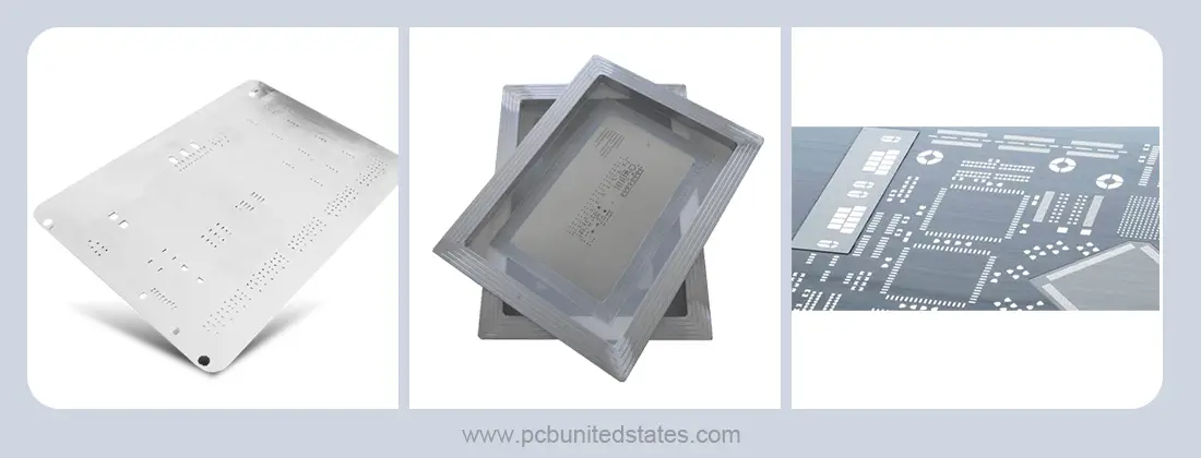
Depending on application requirements of solder pastes, there are three main surface mount stencil types that are typically used:
Framed Stencils
These stencils feature a laser-cut sheet secured within a metal framework, creating a ready-to-use assembly. The frame construction offers increased structural strength and repeatability, which makes these stencils suitable for large-scale manufacturing facilities. The frame also eases the alignment between the PCB and stencil, thus making the process faster. Nevertheless, the added structure increases the initial cost and requires more storage space. The extra weight also raises transport costs, and the frame adds complexity to handling operations.
Frameless Stencils
Frameless stencils, as the name implies, lack the metal frame and are thus a cheaper alternative to framed ones. These lightweight stencils are easy to ship and ideal for small-scale production runs, prototypes, and one-time project applications. They are size-flexible and can be adapted to particular PCB layouts since they do not require frame support. Although less costly, frameless stencils retain their accuracy in applying solder paste as long as they are properly aligned with the circuit board.
Stepped Stencils
In some PCB designs, the various components need different amounts of solder paste. Regular laser-cut stencils are of uniform thickness, and do not provide much control over paste volume. This problems are overcome with stepped stencils, which provide areas of varying thickness in the same stencil. This enables the deposition process of solder past to be controlled very accurately on components with different requirements to enhance the quality of soldering process and overall assembly reliability.
Three Methods to Manufacture Stencils
There are three primary techniques used to produce PCB stencils: chemical etching, laser cutting, and electroforming:
| Methods | Process | Pros | Cons |
|---|---|---|---|
| Chemical Etching | Apply mask → UV exposure → Remove unexposed areas → Etch exposed metal → Clean & inspect |
Cost-effective for simple patterns Well-suited for prototypes and small-batch production |
Precision is limited for fine-pitch designs Aperture walls may end up slightly tapered |
| Laser Cutting | Load material → Input design → Laser cuts apertures → Clean & inspect |
Excellent accuracy and consistency Handles fine-pitch and complex layouts Faster production speed |
Requires costly equipment May cause minor heat effects near apertures |
| Electroforming | Create mandrel → Electroplate metal → Remove stencil → Clean & inspect |
Very smooth and precise apertures Best for ultra-fine pitch components Superior solder paste release performance |
More expensive than other techniques Generally limited to thinner stencil designs |
How to Apply SMT Stencil During the PCB Assembly Process?
Stencil application is a key method to have a successful deposition of solder paste and high quality assembly. This procedure can be broken down into 7 key steps:
Step 1: Prepare the PCB
Ensure that the circuit board is clean of any dust and it is securely fastened in its position to avoid any movement throughout the printing process.
Step 2: Set Up the Stencil Printer
Set up the parameters of a printing machine including speed, pressure, and separation rate. Use fiducial marks or tooling holes to accurately line up the stencil with the PCB.
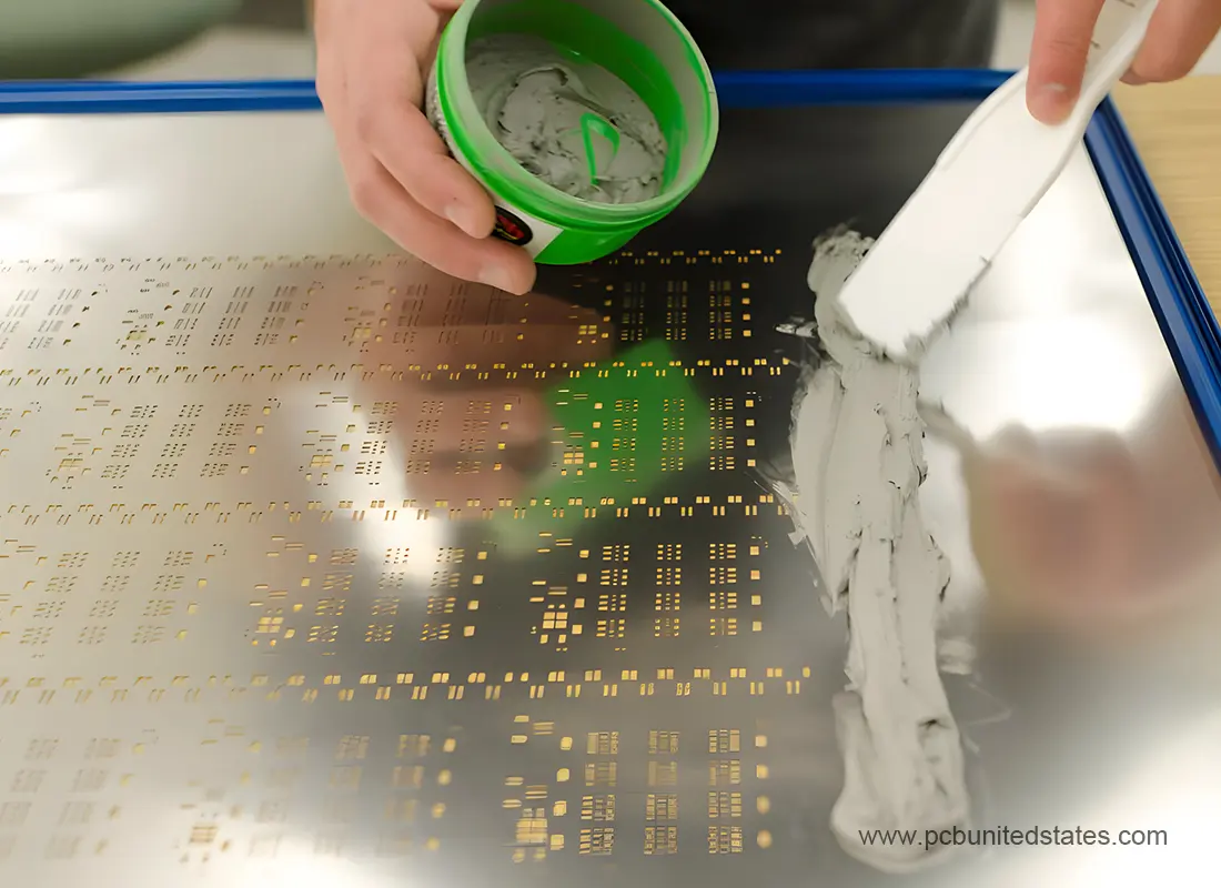
Step 3: Apply Solder Paste
Apply the required amount of solder paste onto the stencil, then spread it uniformly across the surface with a squeegee.
Step 4: Printing Stroke
Move the squeegee across the stencil with a steady force and uniform speed so that all the openings in the stencil are filled completely.
Step 5: Remove the Stencil
Lift the SMD stencil off the board very carefully. This avoids smudging and keeps the solder paste deposits intact.
Step 6: Inspect the Print
Check that the solder paste has been deposited uniformly. For larger production runs, use automated inspection equipment for more reliable quality control.
Step 7: Clean the Stencil
After each use, clear away excess solder paste. Use the proper cleaning method and solution to maintain stencil performance.
To ensure long-lasting performance and consistent results, it’s critical to maintain a stable temperature and humidity at the work place, and check the stencils periodically. More importantly, follow the manufacturer’s guidelines for handling, cleaning, and storage.
How to Choose the Suitable PCB Stencil?
PCB stencils should be carefully selected in order to achieve precise and consistent solder paste placement. There are a number of factors that should be taken into account to make sure that the stencil fits the demands of your assembly process.
Stencil Thickness
The thickness of a stencil determines the amount of solder paste that deposits on the pads of PCB. Typical stencil thicknesses are 0.1 mm (4 mil) on ultra-fine pitch parts, 0.12 mm (5 mil) on standard SMT and 0.15 mm (6 mil) on large components or high-power. The thickness to be selected will be decided by the component lead pitch, pad size and shape and the amount of solder paste required.
Aperture Size and Shape
Stencil aperture dimensions and shape have a direct influence on solder paste release and deposition precision. The important considerations are aspect ratio (aperture width relative to stencil thickness), area ratio (aperture area relative to aperture wall area), and the minimum aperture size allowed by the chosen manufacturing method. The correctly engineered apertures will guarantee the right volumes of solder and effective connection.
Stencil Material
The stencil material affects both durability and performance. Stainless steel is the most widely used option, offering reliable performance across a wide range of applications. Nickel is preferred for fine-pitch designs and step stencils, while polyimide is typically used for flexible stencils in prototypes or small-batch production.
Stencil Alignment
Accurate alignment is crucial to ensure solder paste is deposited correctly on each pad. Alignment can be accomplished through the use of fiducial marks with automated systems, tooling holes with manual fixtures, or stencil borders for visual alignment in prototype setups. The right alignment reduces defects and enhances assembly quality.
Our SMT Stencil Manufacturing Capabilities
MOKO PCB has extensive experience in producing high precision SMT stencils by using laser cutting, chemical etching, and electroforming technologies. From framed stencils and frameless stencils to stepped stencils, we can produce them all with premium quality and accuracy. Our competitive prices, quick turnaround, and stringent quality control help us supply high-quality stencil solutions for your prototype and high-volume production needs. Contact us now to get a free quote and experience superior SMT stencil quality that enhances your PCB assembly process.
Contact Us
Got any questions or inquiries? Fill out the form and we will get back to you soon