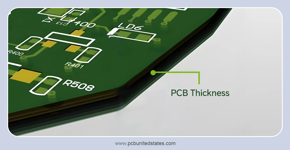
PCB thickness defines the total height of the circuit board, measured from its topmost surface to its bottommost surface, including all layers that make up the complete PCB. These layers include a substrate layer, one or more copper layers, prepreg layers, a solder mask layer, and a silkscreen layer. PCB board thickness significantly affects the board’s mechanical strength, thermal performance, electrical properties, and manufacturability. In this blog post, we will detail the factors that should be considered when determining circuit board thickness. Read on to explore more information!
What Should You Consider When Determining PCB Thickness?
Design Factors
1. Component Weight & Mechanical Stress
PCB thickness can highly affect its mechanical strength. Thicker PCBs have better capacity against physical stress and vibration. Generally speaking, they are more robust and durable, and less prone to deformation or bending. Besides, a thicker board can provide a reliable platform to support numerous and relatively heavy components, especially in a high-density design. When your board needs to install high-power components or multiple heat sinks, consider a thicker PCB. The circuit board gets heavier and less flexible as it gets thicker. Thus, it will need to balance with other factors.
2. Thermal Management & Power Handling
Compared with a thinner circuit board, a thicker one has larger thermal mass, resulting in more effective heat dissipation. In high-power or compact devices, heat accumulation is a severe problem that can impact stable operation. In addition, increasing the copper thickness to 2, 3 ounces or more, can also significantly improve the thermal management.
3. Signal Integrity & High-Frequency Requirements
In high-speed and high-frequency designs, impedance can be affected by dielectric thickness, dielectric constant (Dk), copper thickness, and trace width. The thicker the board, the greater the distance between the trace and the reference layer, resulting in higher impedance. To ensure signal transmission without reflection or distortion, a consistent and controllable impedance must be maintained throughout the entire signal path.
4. Size, Weight, & Space Constraints
PCB thickness is often restricted by the enclosure constraints of the final product. For compact devices such as smartphones, tablets, and wearable devices, a thinner PCB is typically an ideal option. As it’s lighter and more flexible, it reduces weight and space. If space isn’t a constraint, consider a thicker board. It is more robust and durable, but is also heavier and takes up more space.
5. Layer Count & Stackup Complexity
In a multilayer PCB, as the number of layers increases, the overall PCB thickness also increases. For example, a simple double-sided PCB will be much thinner than a complex HDI PCB with 12 or more layers. The stack-up arrangement, that is, the specific arrangement of the copper layers, prepreg layers, and substrate layer, also affects the final circuit board thickness. Also, a circuit board would often be thicker the more copper layers it contains.
6. Copper Thickness & Current Carrying Capacity
The copper thickness is a key factor in measuring the current-carrying capacity and heat dissipation capacity of traces, and it also directly affects the PCB thickness. The standard copper thickness is 1 oz/ft², but for high-power applications, a thicker copper thickness may be required. Heavy copper PCB with 2 or 3 oz copper weight can carry greater current without overheating.
Manufacturing Factors
1. Process Challenges & Limitations
Etching: The thicker the copper layer, the longer the etching time, and the stronger the etchant is required to remove the excess copper. However, prolonged etching time increases the risk of over-etching or under-etching, which can affect the circuit pattern accuracy.
Drilling: The thicker the PCB, the greater the distance the drill bit must penetrate to complete a through hole. Simultaneously, the drill bit experiences higher cutting resistance, increasing the risk of breakage and potentially reducing hole accuracy. Therefore, it often requires specialized drill bits, optimized drilling parameters, and even more advanced drilling techniques.
Lamination Process: Lamination is the process of bonding multiple layers of copper foil and insulating material together under high temperature and pressure. Compared with standard PCBs, thicker PCBs may need longer lamination duration and greater pressure to achieve firm bonding. This also increases the risk of defects such as PCB delamination or warping.
2. Material Availability & Lead Times
For standard PCBs, most manufacturers have a stock of materials, and the supply of materials is sufficient. It means that there will be no delays in material procurement, which will help shorten the delivery cycle. For non-standard PCB thickness, the manufacturer may need to order special core and prepreg materials.
3. Assembly & Soldering
Thicker circuit boards require higher soldering temperatures and longer heating times to ensure proper solder joints. Prolonged high temperatures highly increase the risk of thermal damage, potentially damaging precision components or compromising the PCB’s structural integrity.
4. PCB Depaneling Technique
Depaneling is the process of separating individual circuit boards from a larger PCB panel. Thicker PCBs may require milling or tab routing, while thinner PCBs can be separated using v-scoring, laser cutting, punching, etc. Proper depanelization methods minimize physical stress on the circuit boards and prevent damage during the depanel process.
Is Standard PCB Thickness Always the Right Choice?
1.57 mm is the most commonly used circuit board thickness and is widely considered the industry standard. Below are three main reasons.
- Achieve a good balance between mechanical strength and weight. The circuit board is sturdy enough to endure both production and operation.
- Compatible with most through-hole components. If the circuit board is thicker, the leads may not be long enough.
- Easy to produce. It is easy to handle and not easily damaged, and the PCB board thickness will not cause problems in the production process.
Although 1.57 mm is the standard PCB thickness and suitable for most applications, there are other options. Here are different printed circuit board thicknesses with unique characteristics, making them suitable for various devices.
| Aspect | Ultra-Thin PCBs | Mid-Range PCBs | Thick PCBs |
| Thickness Range | Below 0.6 mm | 0.6 to 1.6 mm | Above 1.6 mm |
| Characteristics | ▪ Extremely thin
▪ Excellent flexibility, easy to bend ▪ Low mechanical strength |
▪ Balanced strength & flexibility
▪ Standard-process manufacturability ▪ Adequate electrical isolation |
▪ Excellent mechanical strength
▪ Better thermal management ▪ Low flexibility |
| Common Applications | ▪ Wearable devices
▪ Medical implants ▪ Flexible displays ▪ Drones |
▪ Smartphones
▪ Tablets ▪ Laptops |
▪ Automotive electronics
▪ Aerospace electronics ▪ Industrial control PCBs |
How to Determine the Right PCB Thickness: A Practical 3-Step Framework
Step 1: Define the Device Scenario
Thoroughly know the end-use environment of your electronic products. The main dilemma is: a thin and flexible design or a robust and durable one? For general electronic devices, a PCB thickness of 0.6-1.6mm may be sufficient. For portable devices, it’s necessary to minimize size and weight. While industrial applications containing high-power components may require thicker PCBs.
Step 2: Analyze Component and Performance Requirements
The next step is to assess the weight, size, and power consumption of the components to be assembled on the board later. Heavier or higher-power components may require a thicker circuit board to provide mechanical support and heat dissipation. Besides, consider the performance requirements of the application, such as electrical performance, mechanical performance, thermal performance, etc.
Step 3: Evaluate Cost and Manufacturability
Finally, assess the impact of the chosen PCB board thickness on cost and manufacturability. Standard PCB thickness is undoubtedly the most economical choice. Using either thinner or thicker boards almost always results in higher material costs and potentially longer lead times. Simultaneously, check the PCB manufacturer’s manufacturing capabilities, including etching, plating, drilling, routing, laminating, and so on.
Takeaway: Is Custom PCB Thickness Available?
Of course! Most PCB manufacturers can provide custom circuit board thickness. Designers can adjust the PCB thickness according to specific application requirements to achieve special performance or functionality that cannot be met by standard circuit board thickness. Different manufacturers may offer different ranges of custom thicknesses.
According to the number of PCB layers, MOKOPCB offers a variety of circuit board thickness options to meet different design needs. Standard thicknesses include 0.8mm, 1.0mm, 1.2mm, 1.6mm, and 2.0mm. Non-standard thicknesses cover 0.3mm, 0.4mm, 0.6mm, 2.4mm, 3.0mm, 3.2mm, and 5.0mm. While the standard 1.57 mm thickness is suitable for a variety of applications, a custom thickness may be the best option in some cases.
