If down your AirPods or computer, you will get delicate green printed circuit boards or PCBs. You may notice that there are various holes on PCBs, but do you know what those holes are and work for? Understanding these circuit board holes is fundamental for PCB design and manufacturing. In this blog, we will have an in-depth look at various PCB hole types, offering you some valuable insights into your actual PCB usage. If you are a PCB beginner or ready for home DIY, this passage is right for you.
| PCB Hole Type | Structure | Functions | Major Types | Drilling Method |
| Through Holes | Holes passing fully through the PCB | Electrical connection, mechanical component bonding | 1. Plated through holes(PTHs)
2. Non-Plated Through Holes(NPTH) |
Mechanical drilling |
| Via Holes | Layer-to-layer plated holes | Electrical interconnection | 1. Blind vias
2. Buried vias 3. Through vias 4. Microvias 5. Stacked vias 6. Staggered vias |
Laser drilling/mechanical drilling |
| Mounting Holes | Non-plated or plated through holes | Mechanical soldering | 1. Plated mounting holes
2. Non-plated mounting holes 3. Countersunk holes 4. counterbored holes 5. Castellated Holes |
Mechanical drilling + milling |
| Special Holes | Depending on the detailed hole structure | Save space, strengthen PCB, breakaway panel, and more | 1. Via-in-Pad
2. Mounting Holes with Vias 3. Stamp Holes |
Laser drilling, mechanical drilling, and more |
PCB Through Holes
A through hole or “thru-hole” on a PCB is drilled from the top layer to the bottom layer of the PCB. Drilling through holes is an old PCB technologies that mainly support lead assemblies, requiring one hole per pin. They almost match two different types: PTH and NPTH. The easiest way to clear these two types of holes is to see whether there are traces of plating on the wall of the hole.
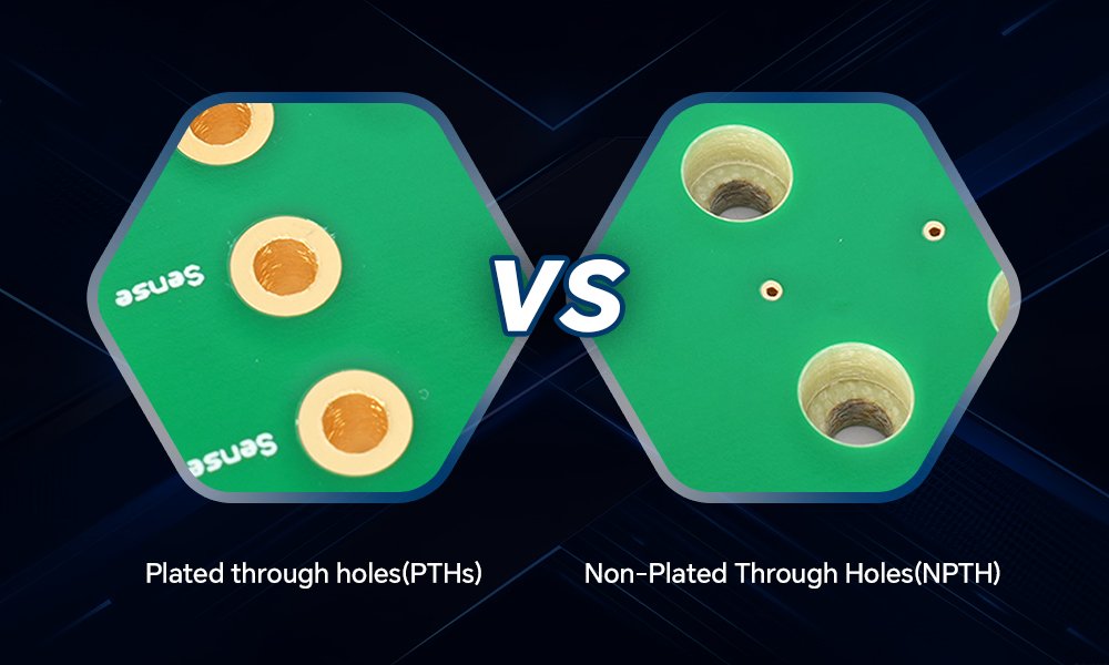
1. Plated through holes(PTHs)
Plated through holes, also called through-hole vias, are holes whose interior wall is plated with a conductive metal layer, typically copper, to establish electrical connections between different layers of the board.
The PTHs mainly work for electrical and mechanical interconnects. When they function as vias in multilayer PCBs, PTHs(typically 0.3–2.0mm) enable signals and power to travel between the entire board(Details in “Through-hole vias). On the other hand, plating through a hole can also be used as a component hole for welding components leads like resistors and capacitors. Such a hole size(1.0-3.0mm) must be larger than the pin of the components so that the components can be inserted into the hole.
2. Non-Plated Through Holes(NPTH)
Non-plated through holes are those holes that remain uncoated with a plating layer, making them purely mechanical in function. We can always see them in a single-layer circuit board, which actually contains no additional copper, so there is no need to plate.
Without an electrical connection, NPTHs are generally used as tooling holes for screws or positioning holes for precise PCB alignment, or venting holes for heat dissipation. Their sizes(1.5-10mm) are larger than PTHs because they lack copper plating.
PCB Via Holes
Vias on PCB are small drilled holes that go through 2 or more adjacent layers. It establishes an electrical connection between layers of a multi-layer PCB. Depending upon their functionality, vias can be classified into 6 types:
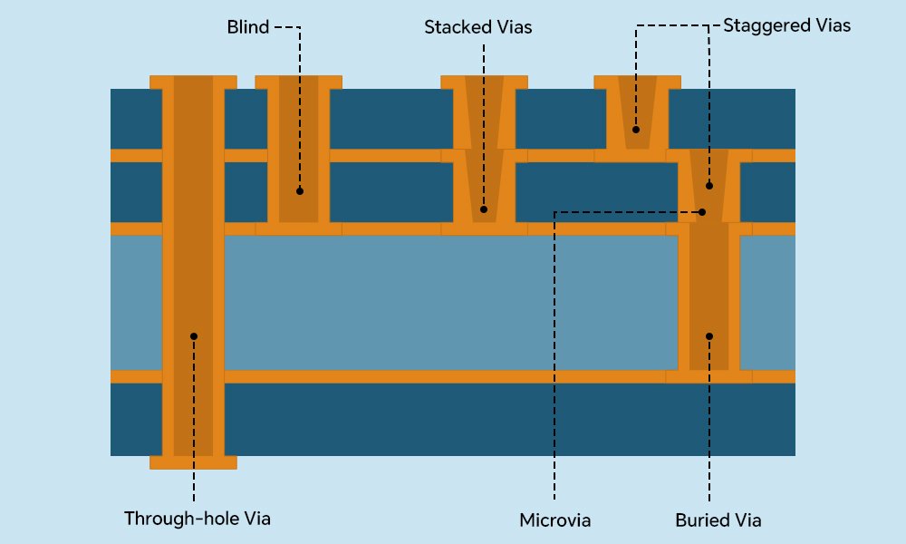
1. Blind Vias
Blind vias extend from the top or the bottom of the board to 1 or more inner layers but don’t pass through the entire board. Therefore, they connect at least 2 layers and need to stop at a specific depth, making them useful for high-density designs with limited space, such as BGA assembling and HDI PCBs.
The general size of the PCB blind via is 0.15-0.3mm. This also causes the requirement for laser drilling or controlled-depth mechanical drilling.
2. Buried Vias
Buried vias are located entirely inside the PCB, connecting two or more inner layers without reaching the outer surfaces. It is designed to transfer inner layer signals, which reduces the chance of signal interference and optimizes routing space.
Invisible on the outer layer, buried vias need to be drilled(0.2-0.3mm) and plated before laminating additional layers, increasing cost and making it suitable for high-speed and HDI PCBs.
3. Through-Hole Vias
Through-hole vias, or PTH, the most common types of vias, span the whole PCB layers from the top to the bottom. When through holes behave as vias, they function for electrical connections.
Through-hole vias are reliable and cost-effective, but take up more space compared to other via types. They are often used in standard PCB designs where the layer count isn’t extremely high.
4. Microvias
Microvias are advanced and small vias used for more advanced and complex printed circuit boards with a smaller surface, like high-density interconnect PCBs. Unlike traditional through-hole vias, micro vias are laser-drilled holes smaller than 0.15mm, which only pass through 1 PCB layer with a maximum aspect ratio of drill depth to drill diameter AR = h/a (perfect for 1:1 and standard for 0.75:1).
If there is enough budget to use movies in PCBs for arbitrarily interconnecting the PCB layers, you don’t need to lay out PCBs painstakingly. Besides, due to their smaller size and shorter signal paths, the microvias reduce parasitic capacitance and improve signal integrity, enhancing the routable area on the board and making it ideal for high-speed PCB designs.
5. Stacked Vias
The stacked vias are actually a type of micro-vias. There are 1 or more microvias stacked on top of each other, forming a continuous conductive path through multiple PCB layers. Each microvia needs to be laser-drilled individually and filled with conductive material, so as to ensure reliability, planting uniformity, and signal integrity.
The primary pros of stacked vias are their compactness, which makes them paramount for devices with super compact PCBs like smartphones.
6. Staggered Vias
Staggered vias are another important type of microvias. The staggered vias connect different layers but are offset from one layer to the next, preventing a straight vertical path. As the second via doesn’t contact the first hole directly, the laser-drilled vias don’t need copper filling. If not, it is prone to take place in thermal stress cracks.
Staggered vias may be a better choice when you want to connect more than 2 layers by microvias because it doesn’t require copper filling and have a lower complexity.
Tips: Different vias can be drilled on a PCB at the same time, such as Blind + stacked vias, buried vias + staggered vias, and more.
| Via Type | Structure | Hole size | Drilling Method | Filling Required |
| Blind Via | Connects the outer layer to the inner layer | 0.15–0.3mm | Laser drilling | Sometimes (if stacked) |
| Buried Via | Connects inner layers only | 0.2–0.3mm | Laser drilling | Sometimes |
| Through-Hole Via | Connects all layers | >0.3mm | Mechanical drilling | No |
| Microvia | Connects 1-2 adjacent layers | <0.15mm | Laser drilling | Sometimes |
| Stacked Via | Multiple microvias stacked vertically | <0.15mm | Laser drilling | Yes (must be filled) |
| Staggered Via | Multiple microvias offset, not stacked | <0.15mm | Laser drilling | No |
PCB Mounting Holes
PCB mounting holes are holes that are drilled entirely through a PCB, which allows the board to be mounted to a chassis, enclosure, or other surface using screws or other mechanical fasteners. Generally, they are positioned at the 4 corners of the board and are drilled with a larger diameter(2.0 mm- 5.0 mm) than other holes. Depending on whether mounting holes have a conductive layer, mounting holes can also be divided into plated and unplated mounting holes.
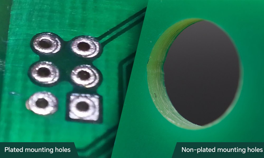
1. Plated mounting holes
Plated mounting holes are mainly used for mechanical fastening and grounding with electrical connections between layers. They mechanically serve as secure anchor points for screws, bolts, or other hardware to make components firmly fixed on the board. Moreover, they are equipped with stronger copper pads for mechanical stability, and the conductive plating also makes them connected to a ground plane for EMI/ESD protection.
2. Non-plated mounting holes
Non-plated mounting holes or tooling holes only function for mechanical fastening and don’t require plating for connectivity. One important point is that the unplated mounting holes are designed to be isolated from other components and traces and need a separate zone to ensure they do not interfere with the other parts’ circuits.
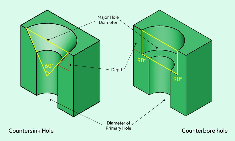
3. Countersunk Holes
Countersunk holes features a conical taper or conical depression, typically at a 90° or 82° angle, which allows lat-head screws to sit flush with the PCB surface, creating a smooth and streamlined finish.
Eliminating protrusions This the countersunk holes prevent interference with other components or mechanical parts while enabling secure screw seating. Countersunk holes are non-plated by default, but selective plating may be used if electrical contact is needed.
4. Counterbored Holes
Counterbored holes are cylindrical holes with a flat bottom and uniform diameter(typically 5–10mm) to accommodate screw heads. They are designed to fully recess hex-head or pan-head screws within the PCB, creating a flat surface.
These holes provide stronger mechanical support than countersunk holes, making them ideal for high-vibration environments.
5. Castellated Holes
Castellated holes or Castellations are indentations created via half-plated, semi-circular edge cuts (0.8–1.6mm diameter), which facilitate direct PCB-to-PCB soldering. Their copper-plated structure acts as SMD pads, eliminating connectors.
Castellated holes are excellent in space savings, simpler assembly, and improved signal integrity for high-frequency modules like ESP32. They’re ideal for modular designs (Raspberry Pi HATs) or stacked boards where minimal height is critical.
PCB Special Holes
Despite common PCB hole types, there are many other special holes on PCBs. Next, we have chosen 3 important ones for you.
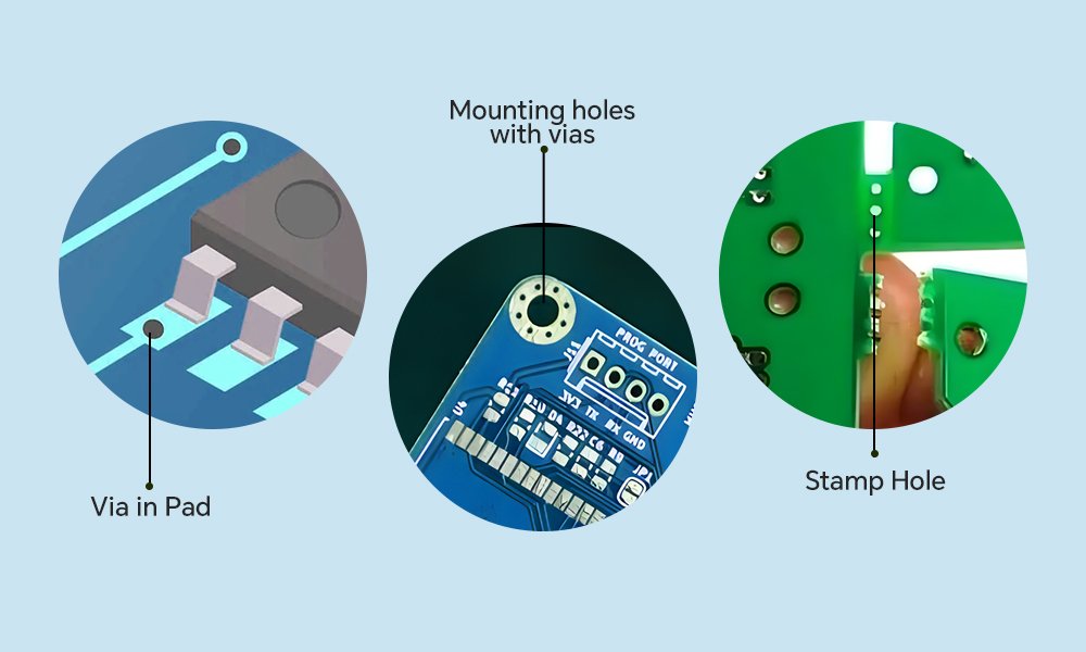
1. Via in Pad
Via in the pad is located within an electronic component pad, drilled to save space and improve signal and power routing. They are super tiny(<0.2mm) and plated with conductive material. Those vias also need to be filled with epoxy/resin to prevent solder wicking.
As a design technology, vias in pads increase PCB density, which is critical for high-density designs like BGA, QFN, or small-pitch ICs.
2. Mounting holes with vias
Mounting holes with vias are those holes where some smaller holes or vias are beside the mounting holes. The vias prevent pad cracking and improve rigidity under mechanical stress. They can also play as thermal vias for heat dissipation, in that vias help transfer heat by creating a path between the PCB and the plane.
Moreover, as we have talked about, vias are mainly used for electrical connections, so those vias also create grounding connections to optimize the grounding paths and reduce electromagnetic interference and noise.
3. Stamp holes
Stamp holes, also called breakaway holes or mouse bites, are closely spaced drill holes along the edge of the PCB within a panel. They are used for PCB breakaway, allowing PCBs to be cleanly removed from a manufacturing panel after assembly.
Their key advantage lies in cost efficiency—they replace V-scoring for thin PCBs and leave minimal residue. However, they’re unsuitable for thick boards (>2mm) due to weaker snap points.
Conclusion
PCB holes are essential for electrical connections, mechanical stability, and thermal management in modern electronics. From PCB through holes to via holes, PCB mounting holes to some special holes, each type of PCB hole serves its unique purpose in PCB design.
At MOKOPCB, we provide various precision-drilled PCBs —— castellated PCB, blind via PCB, stamp hole PCB, and more. MOKOPCB is a professional PCB manufacturer with over 10 years of PCB manufacturing experience. Visit MOKOPCB for reliable and high-performance boards for your project!
