Automatic X-ray Inspection
Nowadays, PCBs are becoming increasingly smaller in size, with components packed more densely on the board. This trend makes quality control even more challenging, and traditional visual inspection has limited capability to detect hidden defects. This is where PCB Automatic X-ray Inspection (AXI) comes into play. This technique has the ability of detecting solder joints that are concealed underneath the package.
What Is Automatic X-ray Inspection?
Automatic X-ray inspection, also referred to as automated X-ray Inspection, is quite a common method of testing to ensure the internal quality and solder integrity of ICs and BGAs in the PCB. Unlike AOI, which uses visible light to scan boards, AXI makes use of X-ray as the scanning source, and thus can scan through the board to reveal internal solder joints, vias, and component terminations without damaging the board.
How Automatic X-ray Inspection Works
To understand how does AXI work, it’s necessary to know the construction of the X-ray inspection machine first. Every X-ray inspection system contains three fundamental elements:
- X-ray tube: It is used to produce the X-ray photons that are required for imaging.
- Platform: The platform is used to hold the boards, which can move in different directions so as to examine the board from different angles and distances.
- Detector: The detector is placed opposite the tube, which is used to capture the transmitted X-ray photons and convert them into a visible image.
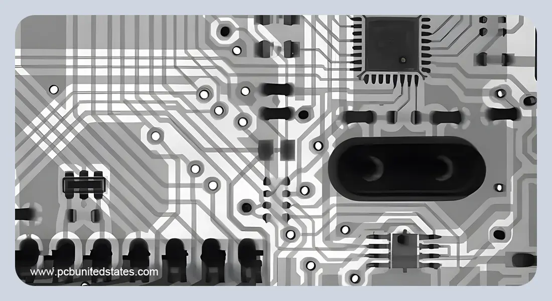
The imaging process operates by passing X-ray photons through the object under examination and collecting them on the other side. The behavior of the photons is determined by the characteristics of the material, such as density, thickness, and atomic composition.
Increased atomic-weight material will absorb more X-ray energy and thus will be more visible in the image, whereas light material will allow more photons to pass through and thus appear more transparent.
Since all materials react to X-rays in different ways, more or fewer photons are received by the detector, forming a contrast that generates the image. The components used in PCBs usually consist of heavier elements and hence are easily viewed in an X-ray image.
Types of X-ray Inspection Machines
The PCB X-ray inspection devices are usually classified into two major categories: whether the system generates 2D or 3D images, and whether it operates offline or online.
- 2D Systems
A 2D X-ray system is a system that generates a two-dimensional image of the PCB, and has a view on both sides of the PCB at the same time. Such a case is likened to a medical X-ray that is employed to identify bone fractures. The 2D systems can operate either off or online due to their simple imaging technique.
- 3D Systems
Conversely, a three dimensional X-ray system develops a three dimensional image of the PCB by stacking a series of 2-dimensional cross-sections. There are two ways of attaining this technique:
Computed Tomography (CT): It is ideal in terms of generating high-resolution 3D images, but can only be done offline because of the intensive algorithms involved.
Laminography: It combines cross-sections to reconstruct specific regions of the board and can either be executed online or off-line.
- Online Operation
Online operation enables the machine to scan boards right on the production line, and information is taken and analyzed in real time. It is suitable for high-volume, complicated PCBs, but the increased capability can slow the processing speed, increasing cost per board and reducing throughput.
- Offline Operation
Offline operation moves inspection off the production line. These tools are faster for sampling or panel checks and are often more economical for smaller batches, though they become less cost-effective as production volumes grow.
AOI vs AXI: Understanding the Differences
Automated Optical Inspection (AOI) and Automated X-ray Inspection (AXI) are both commonly used PCB testing methods, but they use different images sources: AOI uses light while AXI uses X-ray. AOI can only detect the defects on the board surface while PCB automatic x ray inspection can detect internal and hidden issues. The table below shows the types of defects each method can detect:
| Defect Type | AXI | AOI |
| Lifted lead | ✓ | ✓ |
| Faulty component | × | ✓ |
| Missing component | ✓ | ✓ |
| Incorrect component value | × | ✓ |
| Misaligned / Misplaced part | ✓ | ✓ |
| Open circuits | ✓ | ✓ |
| Solder bridges | ✓ | ✓ |
| Solder shorts | ✓ | ✓ |
| Insufficient solder | ✓ | ✓ |
| Solder void | ✓ | × |
| Excess solder | ✓ | ✓ |
| Solder quality | ✓ | × |
| BGA shorts | ✓ | ✓ |
| BGA open-circuit connections | ✓ | × |
Benefits & Limitations of Automated X Ray Inspection
Although Automatic X-ray Inspection has advanced capabilities in checking hidden PCB defects, it also comes with some challenges. Getting familiar with its advantage and limitation assists the manufacturers to determine how to incorporate AXI as part of their inspection process.
Benefits of AXI
- Non-Invasive: X-ray inspection is a non-destructive technique, which enables boards to be inspected without damaging the parts.
- Fast: AXI provides significantly faster inspection speed than detailed manual or visual inspection.
- Comprehensive: It can analyze a variety of quality issues at the same scan including solder bridges, solder joints, pin-hole fills, and solder voids.
- High-Resolution: Advanced imaging offers clear and detailed views of internal structures, which can detect the PCB issues with high accuracy.
- Comparable: Images of the same board may be saved and compared over time to identify the changes or irregularities.
Limitations of AXI
- High cost: AXI systems are costly to purchase and maintain because of the initial investment in X-ray sources, detectors, shielding and specialized software and maintenance costs.
- Slower inspection times: Each board usually requires 1-5 minutes to be inspected, therefore, it is not very conducive to high production volumes unless there are a number of machines to carry out the inspection process.
- Higher operational and safety requirements: Operating X-ray equipment requires radiation safety measures, restricted access, employee training, and compliance with regulatory standards.
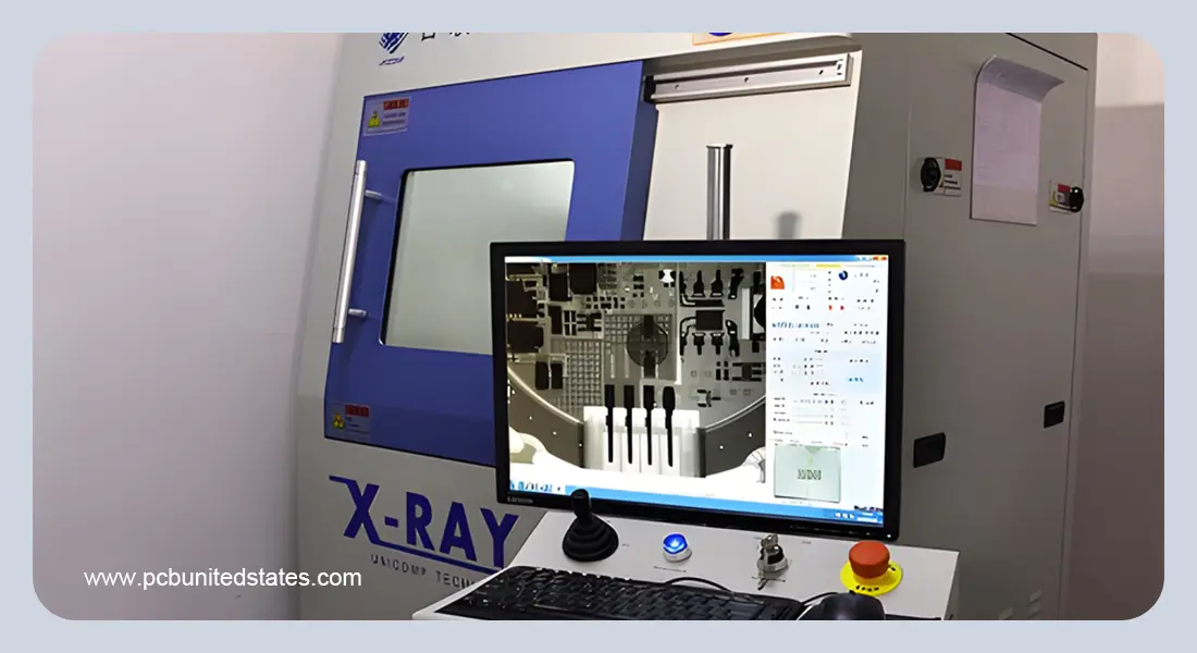
X-ray Inspection at MOKOPCB
X-ray inspection is one of the most important PCB testing methods that we use to guarantee product reliability. At MOKOPCB, our factory is equipped with state-of-the-art x-ray inspection machines with high accuracy, our key capabilities include:
- High-resolution microfocus sources for precise BGA and QFN analysis.
- Inline AXI systems that inspect every board immediately after reflow.
- Automated reporting and traceability to support IPC standards.
Whether you need rapid prototyping or high-volume production, MOKOPCB’s AXI process ensures that every board leaving our facility meets the highest reliability requirements.
Contact Us
Got any questions or inquiries? Fill out the form and we will get back to you soon