PCB Back Drilling
Electronic devices are becoming more multifunctional and the signals they have to process are more complex; therefore, ensuring reliable signal transmission is becoming more difficult. And back drilling is an effective solution that can be used to maintain signal integrity by reducing distortion caused by noise, crosstalk, and via stubs.
What Is Back Drilling in PCB?
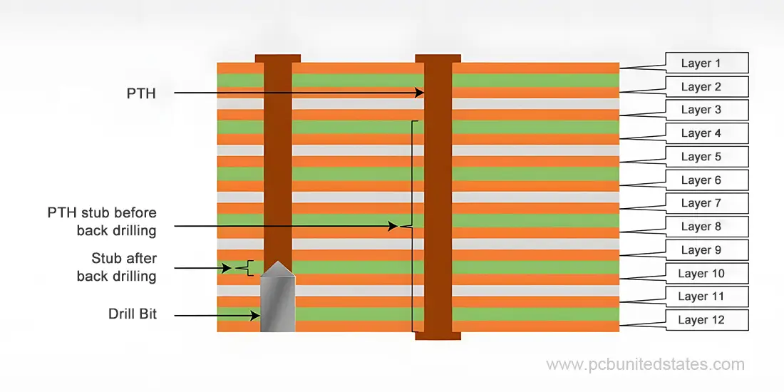
Back drilling is a process employed during the production of multilayer PCBs to remove the unused part of the through holes(known as via stubs), from the inner layers. These stubs are remaining parts of plated through holes that can interrupt the signal transmission by causing reflections and impairing signal integrity. Through drilling out these unwanted portions, back drilling serves to maintain the impedance consistency and decrease signal distortion. This technology is especially useful in high-speed PCB designs, where clean signal paths are essential.
Example
To better understand this technology, let’s take a 12-layer PCB as an example. In this circuit board, a plated through-hole extends from the 1st to 12th layer, but the design only requires electrical connection between the 1st and 9th layers. Therefore, layers 10 to 12 are the unused portions that should be removed by back drilling. After drilling out this portion, the signal performance of the board would be improved.
Benefits of Back Drilling
The following are some of the key benefits that back drilling technology provides:
Minimizes signal reflection and interference: Through the removal of via stubs (part of the via holes that are not intended to carry signals), back drilling can eliminate sources of signal reflection, ringing and electromagnetic interference. This makes the signal transmission cleaner with reduced distortion.
Improves signal integrity and reliability: When via stubs are removed, impedance will become uniform between vias and traces, limiting the possibility of having mismatches that can disrupt signal integrity. This brings to a more reliable PCB performance particularly at a high-speed application.
Enables high-speed performance: The minimized signal degradation enables PCBs to work at higher frequencies and with more accuracy, so they can be used in more advanced systems such as servers, routers, and RF circuits.
Manufacturing Process Overview
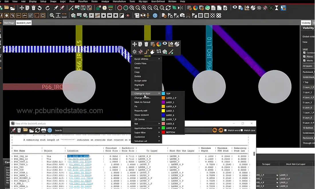
During the back drilling process, a CNC drilling machine is employed to eliminate the via stubs from the reverse side of circuit boards. Generally, the hole created during back drilling is 4 to 6 mils larger than the original one. Usually, the procedure includes the following steps:
- Creating the Via: The first step is to create a standard plated through-hole in the board.
- Defining Drilling Depth: Depending on which internal layers need to be connected, the engineers calculate the depth of drilling required.
- Stub Removal: Special CNC equipment is used to drill the unused part of the via with high
- Precise Depth Control: Advanced systems make sure the drill stops at the right layer, without damaging the essential electrical connections.
When to Use Back Drilling in PCB
Though back drilling helps to improve signal integrity, this technique is not suitable for all PCB designs. It is only necessary in certain situations as listed below:
High-speed designs: Back drilling is required in case of high-speed signals on PCB. It minimizes reflection and ringing of the signal paths by removing the via stubs, hence improving the signal quality.
Dense PCB designs: When the circuit is densely populated with components and space is limited, it can be especially useful. By removing the unused portion of a via, back drilling can free up additional space for other components.
Meeting design requirements: In some cases, back drilling is required in order to meet specifications. For example, if a specification needs controlled impedance and a minimum stub length, back drilling can help achieve both.
Factors Affecting Back Drilling Effectiveness
Before incorporating back drilling into your PCB design, it’s essential to evaluate several factors that impact its performance:
PCB material: The effectiveness of the back drilling would be affected by the PCB material. For example, commonly used FR-4 material is easy to drill, while other materials like ceramic or metal-core boards would require different drill bits and parameters as they are tougher.
Via size and spacing: The size and the spacing of the vias may also affect the effect . Smaller vias need more accurate drilling, whereas larger ones may need bigger drill bits or multiple drillings.
Drill Depth Accuracy: High precision of drill depth is necessary to eliminate via stubs completely without damaging signal layers. When drilling is too shallow, it leaves stubs; when it is too deep, it damages inner layers. Hence, a high-precision CNC machine that has Z-axis compensation and depth control is essential to ensure tight tolerances – typically within +/- 0.05 mm.
Essential Design Guidelines
- Use a back drill chart:Back drill charts assist designers to find the right drill depth and diameter to use on every signal layer. This can eliminate back-drilling mistakes that may result in signal deterioration and signal loss.
- Select an appropriate back-drilling technique: Back-drilling can be done via many ways, including laser ablation, mechanical drilling and plasma etching. Eachprocesses has its benefits and limitations, so it’s critical to choose the one that best fit your design.
- Keep sufficient board margins:During the back drilling process, the vias should keep sufficient distance from board edges to avoid problems like drill bit breakage or or potential damage to the circuit board
- Use controlled impedance routing:Controlled impedance routing can be applied to prevent signal reflections and maintain signal integrity, which is especially critical when using this technique on high-speed signal lines.
- Minimize back-drilled via count:Back drilling is a time-consuming and costly process; therefore, designers should endeavor to reduce the number of back-drilled vias. This is possible through the proper selection of the layer stack-up and utilization of blind and buried via.
Partner with MOKO PCB for Advanced Back Drilling Solutions
Back drilling has become an indispensable technique in modern PCB manufacturing, enabling designers to achieve optimal signal integrity in high-speed applications.
MOKOPCB has vast experience in manufacturing multilayer PCBs, and we specialize in carrying out accurate back drilling based on the requirements of your design. Whether your application uses high speed digital circuits, dense component layouts, or tight performance requirements, we have the capability to provide the best results.
Are you ready to talk about your PCB project? Fill out the form below to submit your requirements and our team will tailor a solution for you.
Contact Us
Got any questions or inquiries? Fill out the form and we will get back to you soon