Zero PCB is a popular choice for quickly and affordably prototyping and testing circuits. Compared with a standard PCB with predefined layout, the Zero PCB board offers maximum design flexibility. In this blog, we’ll walk you through how to build basic circuits on Zero PCBs – from planning the layout to soldering and testing.
What is Zero PCB?
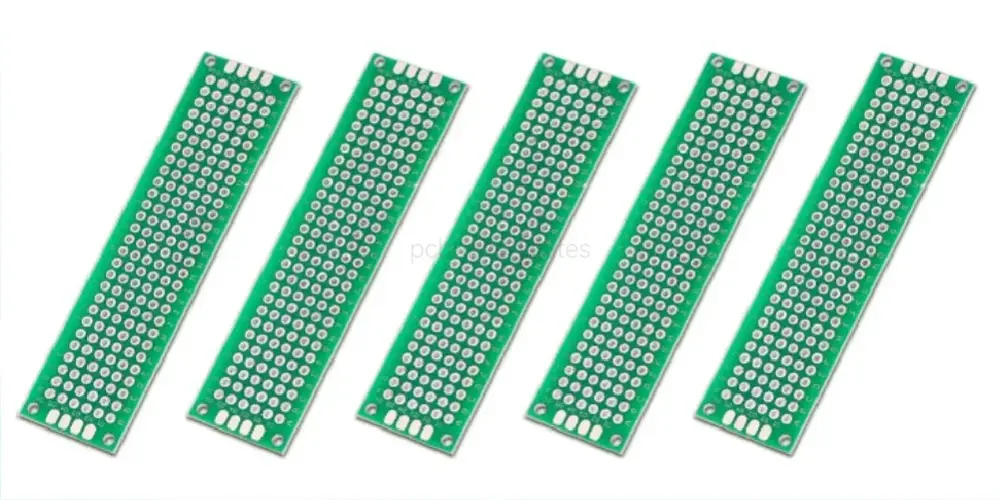
Zero PCB, also known as Dot PCB or Perfboard, is a versatile and general-purpose board without pre-designed PCB traces and pads. There are many small holes laid out in a grid on the zero PCB board. Each hole is surrounded by its copper pad, electrically isolated from the rest. Unlike standard PCBs, this type of PCB usually does not have a solder mask and silkscreen layer. With a simple and basic structure, a zero circuit board is a convenient platform or blank canvas for designing a custom layout, allowing for quick prototyping, testing, etc.
How to Build Basic Circuits on a Zero PCB: A Step-by-Step Guide
Now that you know about the basics of Zero PCBs, let’s see how to build simple circuits on the board.
Step 1: Prepare Tools and Materials
You should prepare everything you will need to ensure the process goes well. Here we list some tools and materials you may need.
Tools: Soldering iron, solder wire, wire cutter or stripper, multimeter, etc.
Materials: Zero PCB, electronic components (resistors, capacitors, etc.), jumper wires, flux, solder, etc.
Step 2: Plan the Circuit Layout
First, draw your circuit diagram on a sheet of paper (or PCB design software). You can consider placing the related components together. Decide where you will place each component on the zero PCB board and avoid overlapping wires.
Step 3: Insert Components
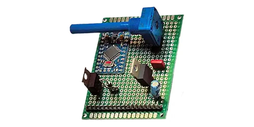
Insert the components onto the zero board as per your circuit diagram. Then, bend the leads a little to hold the component in place. Finally, recheck the orientation of electronic components (e.g., polarized ones).
Step 4: Solder the Components
Turn over the zero PCB board. Use the soldering iron to heat the lead and pad, then apply solder to create a robust bond. If needed, you can apply flux to enhance solder flow and create solid connections. Ensure clean and solid solder joints, avoiding cold solder or solder bridges. After a soldier is made, cut off excess leads using a cutter.
Step 5: Wire Electrical Connections
The components can be connected with bare copper wire or insulated wire. When choosing insulated wires, you need to strip them of insulation at either end. Then, cut the wires to the correct length and solder the two ends to the proper pads. For longer runs, you can use jumper wires on the front or back of the board to avoid complex wiring.
Step 6: Test the Circuit
In completing the above procedures, carry out the test to ensure the zero PCB run as anticipated. You can verify voltage levels and trace connections with a multimeter.
10 Pro Tips to Make Reliable Circuits Using Zero PCB Board
Don’t let small mistakes ruin your circuit. In this part, we summarize 10 pro tips to help you successfully make reliable circuits on the zero printed circuit board.
Start with Layout Planning – Plan your layout upfront to avoid complex and unnecessary wiring and reduce errors. Ensure proper spacing and alignment for easy soldering. For more complex circuits, modularize your circuit into sections.
Group Related Components Together – Placing components that work together near each other keeps your layout cleaner and easier to wire.
Apply Flux for Better Solder Joints – Use flux to increase solder fluidity, resulting in strong and reliable solder joints and connections.
Avoid Overheating – Do not leave the soldering iron heated for long periods of time, as this can easily overheat to damage components and copper pads.
Practice Soldering Technique – When soldering, be quick and gentle for the best results. As for beginners, you had better practice soldering techniques.
Trim Leads After Soldering – After soldering, trim the excess components’ leads to keep the zero PCB clean and avoid short circuits.
Wiring Best Practices – Keep wires short and direct to minimize resistance and short-circuit risks. If needed, use color-coded wires for easier debugging.
Test as You Go – Don’t construct the entire circuit at once. After completing a section, test it to ensure everything works as it should. It is much easier to catch errors early than to debug them afterward.
Verify Before Powering On – Always double-check connections before powering on. The circuit may malfunction due to a simple error.
Label Your Circuit – Labeling the critical components and wires. This can make the following testing, upgrading, and troubleshooting easier.
Pros and Cons of Zero Printed Circuit Boards
Pros of Zero PCB
Easily Accessible and Low Cost
Zero PCBs are inexpensive and readily available. This is an ideal choice for hobbyists or projects with a limited budget. The board can be reused and redesigned for different projects.
Highly Flexible for Prototype
With Zero PCB, you have maximum flexibility in prototype circuit design, determining the layout and connection of each component. If any issues arise, you can quickly modify the design and make adjustments flexibly.
Perfect for Quick Testing and Iteration
Rapid testing and iteration are made possible by Zero PCB, which can speed up the development process. This helps reduce the need for redesign, remanufacturing, and retesting per iteration, while lowering overall costs.
Prototyping for Enclosure Fit
The Zero PCB board makes it simple to estimate and adjust the mechanical cover’s size for the ideal fit. If you measure the cover size with a tape measure, the result may not be accurate enough.
Cons of Zero PCB
Labor-intensive Assembly
Zero PCB boards have no pre-designed circuits or pre-defined component positions, requiring manual assembly. Engineers also need to be proficient in soldering techniques for various components.
Limited Circuit Complexity
Zero boards are not suitable for high-frequency or complex circuit designs and are often used to test and verify partial circuits.
Poor Long-Term Reliability
These boards are not designed for use in harsh environments and may have risks with wire connections being poor or broken.
Typical Applications of Zero Circuit Boards
Circuit Prototyping and Testing
Zero PCB is commonly used for prototyping and evaluating circuit designs before finalizing a custom PCB layout. It is perfect for trial-and-error during early development stages.
Educational Projects and Learning
In school, zero printed circuit boards are a popular tool. They can be used by educators to instruct pupils in circuit design and construction. Students can also learn to solder and wire.
Hobby Electronics and DIY Projects
Due to its affordable price and flexible design, the zero circuit board is very popular among DIY enthusiasts and makers. Any creative idea can be built on it.
Conclusion
This blog has covered circuit construction using a zero PCB. It is economical and used in rapid testing and prototyping. Nevertheless, zero PCB boards are not very suitable for mass manufacturing. Are you willing to transform your prototype into a professional PCB? MOKOPCB is your trusted partner! We have almost 20 years of experience in the PCB and PCBA industry, allowing us to provide custom and high-quality PCBs. Contact us for more information.
Zero PCB FAQ: Clarifying Common Doubts
- What is the difference between a zero PCB, breadboard, and bare PCB?
Zero PCB: A general-purpose board with isolated holes and copper pads. Need manual wiring and soldering.
Breadboard: This is a reusable plastic board used for quickly conducting circuit experiments without soldering.
Bare PCB: A blank PCB without any installed components, including substrate, copper trace, solder mask, and silkscreen.
- How thick are zero PCBs?
The zero PCB boards are usually between 1.2mm and 2mm in thickness, with most being around 1.5mm to 1.6mm.
- What are the sizes and shapes available for zero PCB boards?
Zero PCBs come in square, rectangular, and round shapes. Sizes vary from small (like 5×7 cm), medium (like 10×15 cm), to large (up to 30×30 cm).
- What materials are frequently used to make zero boards?
Zero PCB can be made of various materials depending on your project requirements, such as FR1, FR4, and Polyimide.
- Is it possible to reuse a zero printed circuit board?
Yes! You can reuse the zero PCB board if all the components are stripped from it.
