Why PCB trace width matters? Calculating the size of PCB traces is one of the most fundamental considerations in PCB routing. The width of intricate traces directly impacts the performance, reliability, and safety of the circuit. That’s why PCB designers turn to professional industry standards to guide the trace width calculation. Among them, IPC standards are the most widely used. In this blog, we will lead you to explore how to calculate trace width of PCB based on two major IPC standards(IPC-2221 and IPC-2152) and give you an insight into how to choose between them.
What is IPC standard?
IPC standards are a series of industry-recognized guidelines developed by IPC (Institute of Printed Circuits), a global trade association for the electronics industry. These standards are used to design and manufacture electronic equipment and circuit boards to ensure product quality, reliability, and consistency. Adhering to these standards can reduce the communication gap between designers and manufacturers.
In printed circuit board design, IPC-2221 and IPC-2152 are two major types of standards that provide a framework for designing reliable and safe PCBs. They are widely recognized in the electronic industry and used as a reference by PCB designers and engineers.
How to Calculate Trace Width of PCB Based on the Use of IPC 2221?
The IPC 2221 standard is an industry guideline for generic PCB design and helps PCB designers to quickly determine the trace width required to safely carry current. The IPC-2221 standard defines the current-temperature relationship with a formula, which can output cross-sectional area and trace width.
IPC 2221 empirical formula:

Rearrange the formula to get the formula of cross-sectional area(A):

Cover A to trace width based on:
A=Trace Width (W)×Copper Thickness (T)
So, the core formula of trace width(W) should be:

I = Current in Amps
ΔT = Allowed temperature rise in °C
A = Cross-sectional area of the trace (mil²)
k, b, c = constants that differ for internal and external layers
| Trace Type | k | b | c |
| External | 0.048 | 0.44 | 0.725 |
| Internal | 0.024 | 0.44 | 0.725 |
What needs to be noticed is to keep the units consistent. If the cross-sectional is measured in mils, use mils for trace width and thickness. The path thickness is typically measured by its weight with a unit of oz/ft².
1 oz/ft² copper ≈ 1.37 mil ≈ 35 µm
1 mil = 0.0254 mm
Gather Parameters
Measure the maximum current(I) that the trace can carry. Higher current requires wider traces to avoid overheating. The maximum current rating depends on the conductor material(copper has a lower resistivity than aluminum, which means higher current capacity), cross-section(Thicker conductor means lower resistance and higher current capacity), cooling conditions(reduce temperature rise), and other key factors.
ΔT is the temperature allowed to rise above the surrounding environment, which helps you set a safe limit. Concrete temperature rise is impacted by multiple factors, including specific application requirements, trace materials, open or enclosed environment, and copper thickness. Typical ΔT choice ranges from 10℃ to 40℃, depending on specific requirements. 10℃ is the most common one for general-purpose PCBs.
Copper thickness directly impacts the trace resistance and current capacity. According to the formula = Length of conductor, A(Cross-sectional area = Width × Thickness), Common PCB copper thickness weights are 0.5 oz, 1 oz, 2 oz, 3 oz, and more.
Realistic Example
If choosing the next parameters for the IPC-2221 calculator:
Current(I): 2A
Temperature rise(ΔT): 10℃
Copper thickness(T): 1oz(1.37mil)
Trace layer: External
Cross-sectional area:

Trace width:
W= 150mil²/1.37mils≈110 mils(≈2.8mm)
Here, the trace width formula based on IPC 2221 standard only considers the parameters of cross-sectional area(copper thickness), current, and temperature rise. Trace width calculation can be further defined according to different considerable factors, such as resistivity, via holes, differential pairs, or high-density designs. For different considerations, the trace width formula varies.
How to Calculate Trace Width of PCB Based on the Use of IPC 2152?
IPC 2152, also called “Standard for Determining Current-Carrying Capacity in Printed Board Design,” is a comprehensive industry standard. It provides guidelines for determining suitable internal and external trace width based on current and allowable temperature rise. It also indicates how key factors like copper thickness, PCB environment, airflow conditions, and material affect the trace width calculation.
Choose the correct IPC 2152 chart to find the precise cross-section or trace width based on the confirmed parameters. IPC2152 contains families of curves: X-axis: Cross-section/Trace width (mils or mm); Y-axis: Current (A); Curves: Different temperature rises. Locate parameters on the chart and read the cross-section for the trace, and then calculate trace width based on the formula W = A/T, and make sure A and T are in the same units (mil² and mils, or mm² and mm) when converting.
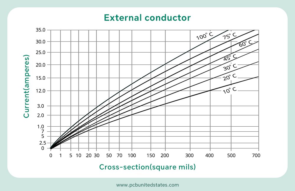
The key charts are Figure4-1, Figure 4-2, and other charts for different copper weights. Figure 4-1 is used for external layers with better heat dissipation, and Figure 4-2 is for internal layers with worse heat dissipation.
How to access the authoritative IPC2152 charts? The most authoritative source is to purchase the official IPC-2152 standard document, which is protected from copyright, from the IPC website. The document provides detailed charts and guidelines to confirm cross-section and trace width.
IPC 2221 VS IPC 2152: Use Which One?
IPC 2221, published in 2003, is an older standard than IPC2152 in 2009. It is based on empirical curves from laboratories on simple boards, so it always deals with simple PCB design, but is not good at solving high-density boards or complex thermal situations. On the other hand, IPC 2152 is a more advanced standard based on extensive empirical testing, so it is practical to address modern and more accurate PCB needs with experimental data and simulations, like high-current PCBs(motor drivers).
As for accuracy, IPC 2221 only provides a basic formula for trace width based on current and temperature rise, leading to a more conservative result for trace width. IPC 2152 is more detailed with more real factors taken into consideration, such as trace layout and ambient temperature, providing more accurate calculations.
Regarding temperature rise, IPC 2221 linearly treats the heat rise with a single parameter is considered in the allowable temperature rise. However, IPC 2152 accounts for multiple factors that may affect temperature rise, such as trace materials, layer counts, copper thickness, realistic ambient temperature, and more. This brings about a more precise and generally smaller trace width result.
| Feature | IPC-2221 | IPC-2152 |
| Formula | I = k * (ΔT)^b * A^c | Detailed charts & calculators based on data & simulation |
| Purpose | General PCB design, simple trace width calculation | Modern, detailed PCB design, accurate trace width & ampacity |
| Basis | Empirical formula from lab tests | Experimental data + thermal simulation |
| Temperature Rise | Single ΔT for allowed rise | Considers thermal conduction, ambient, multi-layer effects |
| Trace location | Internal vs External (simple factor) | Internal, External, plus layer depth, copper distribution, proximity effects |
| Accuracy | Conservative, may oversize traces | Accurate, optimized for real-world conditions |
| Use Case | Simple boards, early-stage design | High-current, dense, multi-layer, professional boards |
| Ambient conditions | Limited consideration | Various ambient conditions |
Conclusion
Now, you must have a comprehensive about how to calculate trace width of PCB based on IPC-2221 and IPC-2152 standards. The IPC-2221 calculator offers a simplified formula-based way for conservative trace width results, practical for simple printed boards, and IPC-2152 delivers a more detailed and advanced method based on realistic testing for more precise and modern results. Understanding two standards brings you flexibility to design PCBs with confidence. MOKOPCB highlights these PCB trace design considerations and fabricates high-precision PCBs with advanced manufacturing capabilities. Freely contact us, and our team ensures every board delivers the best performance for your projects.
Read More:
