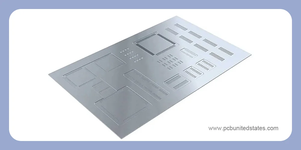
SMT (surface mount technology) is a core technology in PCB assembly. As placement accuracy and component density keep rising, solder paste printing demands greater precision. PCB stencil directly determines the consistency and reliability of solder paste printing. The stencil is commonly a piece of stainless steel with designed openings. It’s used to deposit solder paste to the SMT pads accurately and precisely, which can significantly increase the efficiency of the assembly process. While choosing the right stencil for surface-mount assembly, you should consider some critical factors. Learning from this blog can clear all your confusion.
Key Factors to Consider When Selecting a PCB Stencil
In this part, we will list some key factors that may influence the PCB stencil selection. Considering them thoroughly can help you choose the ideal SMT stencil, ensuring accurate solder paste deposition and reliable assembly results.
Production Scale and Board Complexity
For large-scale production and complex PCB design, it’s recommended to choose a framed stencil. If you are working with small-scale production, prototyping projects, or a simple board, it’s suitable to select a frameless stencil or prototype stencil, which is a cost-effective option.
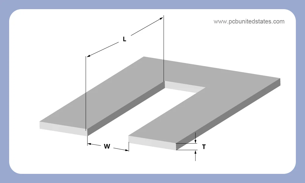
SMT Stencil Thickness
The thickness of the PCB stencil is a critical parameter, usually ranging from 0.08 mm to 0.2 mm. It affects how much solder paste is applied to the pad. The suitable amount is key to achieving reliable component solder joints. Excessive solder deposition may cause solder bridging, but insufficient solder deposition can also result in weak solder joints. Moreover, the stencil thickness is also determined by the smallest component’s pitch.
Aperture Size and Shape
 Typically, the aperture size is smaller than the pad size, avoiding the excess solder paste. For standard components, the aperture-to-pad ratio is 0.9. For finer pitch components (less than 0.5 mm), the ratio should be reduced to 0.8 to minimize the risk of solder bridges. Aspect ratio is also important, typically maintaining between 0.66 and 1.5.
With QFNs, the stencil aperture shape sometimes needs to be adjusted to accommodate a windowpane design, which divides the aperture into many smaller segments. This design can achieve a 30% reduction in voiding rates relative to a single large opening.
PCB Stencil Material and Construction
The capacity of the PCB stencil to transfer solder paste from the opening to the SMT pad is influenced by the materials used. Stainless steel is commonly used to produce the stencil. It offers outstanding durability, easy-to-clean, and corrosion-resistant properties needed for frequent use.
However, you can also choose other materials, such as nickel and brass. While nickel is less commonly used than stainless steel, it is famous for its flexibility and wear resistance. SMT stencil’s durability will also be impacted by its construction. The electroformed stencil offers both high durability and excellent printing accuracy, making it an ideal choice.
Type of Solder Paste
The type of solder paste applied will influence stencil selection. Different kinds of solder paste have various properties, like particle size and viscosity. With fine-pitch components, the finer powders would be better. Viscosity determines how solder paste flows across the stencil and releases into the apertures.
Common Mistakes in PCB Stencil Selection and How to Avoid Them
Choosing the right PCB stencil is critical for ensuring success and a smooth SMT assembly process. However, it’s easy to make mistakes during the selection phase. Here are some common mistakes you might face.
1. Treating “0.12 mm” as the Universal Thickness
Many designers and engineers default to a 0.12mm thickness of PCB stencil, which is suitable for all projects. This is not a one-size-fits-all solution, which may result in costly mistakes and finally cause poor solder paste deposition. As we have talked, the optimal PCB stencil thickness should depend on the component’s pitch. Here are some useful tips:
- ICs or BGAs at a 0.35 mm pitch: Use a stencil ≤0.08mm. If the entire board is assembled with these fine-pitch components, a 0.06mm or even 0.05mm SMT stencil is recommended.
- ICs or BGAs ata 4 mm pitch or greater: A 0.08–0.10mm stencil is commonly acceptable.
- ICs or BGAs at a5 mm pitch or larger: 0.12mm stencil is a typical choice.
2. Copy-Pasting the Copper Pad into the Aperture File
Do not simply copy the copper pad dimensions into the PCB stencil aperture file. This is an easy-to-make mistake. Aperture sizes are commonly determined by the component type, pad geometry, and assembly requirements. The apertures should be smaller than the pad size to avoid some soldering defects, such as solder balls and bridges. It’s advised to take time to review and optimize each aperture individually, not just copy the pads to the design file.
3. Picking Laser-Cut Stainless Steel Stencil for Every Project
 Laser-cut stencil uses advanced laser technology to cut openings in stainless steel sheets. This technique allows for precise control of aperture size and shape, achieving micron-level accuracy. For prototypes or low-volume production with larger components, it works well. However, it’s not always the best choice for every project. There are many PCB stencil types available, including framed stencil, frameless stencil, electroformed stencil, chemical-etched stencils, step stencils, etc.
For high-volume production or designs with fine-pitch components, it’s recommended to choose electroformed or chemical-etched PCB stencils, providing superior paste release. With some complex PCBs, it is often necessary to install different components, each with its own specific requirements for solder paste. Laser-cut PCB stencils with a uniform thickness are obviously not suitable. In order to achieve higher soldering efficiency and quality, the step stencil was developed. It has different thickness levels to meet the desired solder paste amount needs.
4. Ignoring the Paste Type to Be Used
Solder paste type is an often overlooked factor in PCB stencil selection. Different solder pastes have varying rheological properties, which directly impact stencil selection. They are a system, so both should be considered simultaneously. The particle size of solder paste is a key factor in determining its suitability for different components. Solder paste can be divided by numbers, such as Type 3, Type 4, Type 5, etc, with lower numbers indicating larger particles.
Type 3 is an economical option and suitable for larger components. Its solder powder particle size range is 25–45 µm. Type 4 or Type 5 solder paste is ideal for miniature components, allowing the use of smaller stencil apertures.
5. Neglecting Board Size and Layout Complexity
Designers often focus on pad design, overlooking how the physical size and complexity of the PCB can significantly influence stencil selection. Large boards may require a framed stencil for proper support and alignment. Smaller boards can opt for a frameless stencil. Dense layouts with varying component heights may require a stepped stencil to accommodate varying solder paste volume requirements. Flexible or rigid-flex boards may come with a unique challenge, requiring specialized stencil design and support.
6. Forgetting Fiducial Marks Until the Quote Is Sent
Many designers focus solely on the apertures, forgetting that the stencil itself also requires fiducial marks for precise positioning. Stencil alignment issues occur when the stencil apertures don’t align perfectly with the PCB pads. This can result in incorrect solder paste deposition, insufficient solder deposits, or solder paste deposits in unintended areas.
7. Buying on Price Alone
While the cost is always the key consideration during the PCB stencil selection, it can not be the only consideration. If you choose a PCB stencil solely based on the lowest price, it often leads to costly problems later on. Cheap stencils may use inferior materials and have poor aperture quality. In the printing process, it’s highly possible to cause inconsistent solder paste printing, increased defects, and ultimately lead to a higher total cost. We greatly recommend choosing a slightly higher-priced PCB stencil that improves yield and reduces rework costs.
Last Words
PCB stencil is crucial for the SMT assembly process. It can accurately control the amount of solder paste deposited and ensure high-quality component soldering. Choosing the right stencil can greatly improve the quality and speed of PCB assembly. If you are looking for a one-stop PCB & PCBA service, MOKOPCB can be your first choice. Since 2006, we have offered seamless integration from design to delivery, providing professional PCB solutions.
PCB Stencil FAQ
Q1: How to manufacture stencils?
A1: There are three main methods to produce PCB solder stencils, including laser cutting (subtractive process), electroforming (additive process), and chemical etching (subtractive process).
Q2: What is the difference between solder paste and solder mask?
A1: The solder paste is a kind of material that is mixed with solder and flux. It’s applied to the pads before placing the components, forming a strong connection between the pads and components. While solder mask is a thin protective layer that covers the circuit board surface except for pads, preventing solder bridging and protecting copper traces from oxidation.
Q3: Why are SMT stencils beneficial for assembly?
Q3: PCB stencils guarantee that solder paste is precisely applied to pads, ensuring a consistent high quality of the solder joint. Moreover, they speed up the assembly process and reduce rework, which is critical for mass production.
Q4: How to clear a PCB stencil?
A4: After using the SMT stencil, it’s necessary to clean it. You can first use a special wiping paper and alcohol to clean the surface and bottom of the stencil. Then clean the openings with a brush and alcohol, moving from left to right and top to bottom.
