An IC Package serves as an enclosure to shield the integrated circuit from external influences, such as moisture, physical damage, and dust. Except for the housing, it also provides an electrical connection. Integrated circuit packaging is just as critical as the integrated circuit itself, both determining the chip’s performance, reliability, and thermal performance in the electronic system. With so many IC package types available, choosing the right IC package can be challenging. In this blog, we’ll introduce the 7 main types and discuss the key factors to consider during the selection.
How to Choose the Correct IC Package?
Selecting the right IC package is crucial because different IC package types can significantly affect the board’s size, heat dissipation, assembly method, and overall performance. The ideal IC package should also strike a balance between cost, performance, and manufacturability. Here are the key factors you should carefully consider when making a decision.
PCB Size and Layout Constraints
Available board space typically determines which IC package should be used. If your design is compact, the CSP is an ideal option. But if space is not an issue, a larger package like a DIP may be easier to handle during prototyping.
Thermal Management
Thermal management is a critical issue, especially in high-power integrated circuits (ICs). The IC package must effectively dissipate the heat generated by the chip to prevent overheating and ensure reliable operation. The package should be designed to have better heat dissipation performance, such as BAG.
Signal Integrity
Pin length and parasitic effects can impact signal integrity. For high-speed or high-frequency circuits, signal integrity is critical. It is crucial to take signal transmission quality and stability into account when choosing a package. QFN packages, with their low parasitic parameters, are an ideal choice.
Performance Requirements
The IC package should align with the chip’s functional requirements. If you require high pin count, advanced IC package types such as QFP or BGA are recommended. If not, simpler options like DIP or SOP packages should be adequate.
Cost Considerations
Simpler IC package (such as DIP or SOP) IS typically less expensive in terms of production and assembly. Although an advanced package may come with higher manufacturing costs, it can help save board size and enhance performance, making it a practical choice for high-density or complex designs. Besides, the cost efficiency of an IC package often depends on production volume. While DIP packages are economical for low-volume manufacturing, surface-mount options like SOP or QFP can provide better cost efficiency in mass production.
IC Package Types Explained
IC packages come in various types, each offering unique properties in size, performance, and thermal management. Understanding these IC package types is essential for selecting the right package for your design.
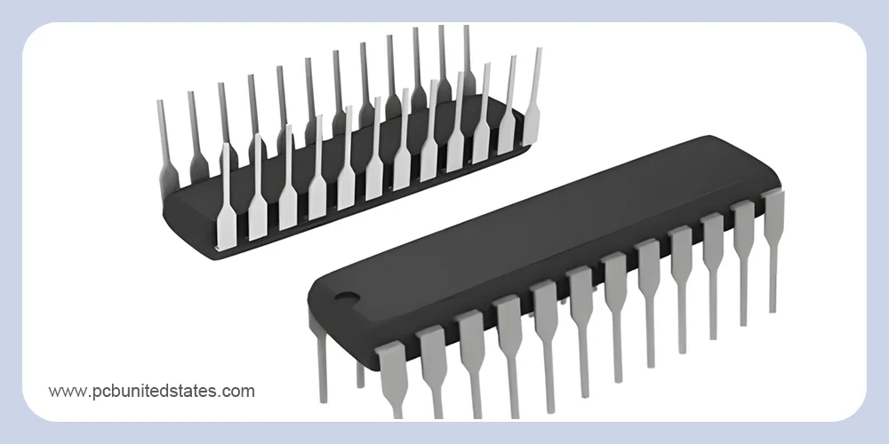
DIP (Dual Inline Package)
The dual inline package IC is a common type of through-hole IC package characterized by two parallel rows of pins protruding perpendicularly from the enclosure. The standard lead pitch of the pins is 2.54mm. Its whole dimension depends on the pin count, which ranges from 8 to hundreds. A DIP IC package can be both directly soldered to the board and inserted through an IC socket.
- Pros: Easy to process and solder, Perfect for low-density applications, Strong bonding connection to the circuit board, Convenient for repair and maintenance.
- Cons: Large physical size, Limited capacity in high-density applications, Prone to cause capacitance and inductance issues, Restricted I/O capability.
- Ideal for: Prototyping, Hobbyist projects, Low-frequency circuits.
- DIPcommon variants: SDIP (Shrink Dual In-line Package)
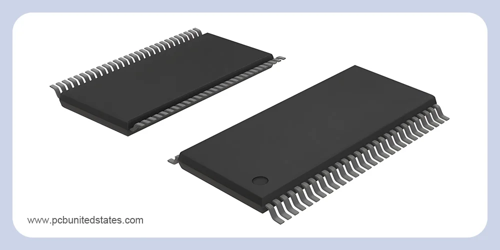
SOP (Small Outline Package)
SOP is a kind of surface-mount IC package, featuring a rectangular body with two rows of “gull-wing” leads on opposite sides. It occupies less space and can be directly soldered on the board surface. SOP shares similarities with SOIC (Small Outline Integrated Circuit), but has different dimensions and pin spacing. The pin pitch of SOP packages is typically 1.27 mm or less.
- Pros: Small physical size, High packaging density, Light weight, Excellent performance, Allows for automated assembly.
- Cons: Limited heat dissipation (compared with DIP), Limited heat dissipation.
- Ideal for: Amplifiers, Memory chips, Miniaturized electronic devices, High-density design, Portable devices.
- SOP common variants: VSOP (Very Small Outline Package), SOJ (Small Out-Line J-Leaded Package), TSSOP (Thin Shrink Small Outline Package), SSOP (Shrink Small Outline Package), TSOP (Thin Small Outline Package), QSOP (Quarter Small Outline Package).
QFP (Quad Flat Package)
QFP has a square or rectangular body, protruding “gull-wing” from its four sides. This type of IC package typically has 32 or more pins. These pins are very fine and arranged in a grid pattern, allowing them to be soldered onto a circuit board using surface mount technology (SMT).
- Pros: Compact footprint, High pin count, Easy to solder and inspect, Ideal for automation, Socket compatibility.
- Cons: Not ideal for high-frequency applications, Limited thermal conductivity
- Ideal for: Consumer electronics, Control systems, Communication devices, Microprocessors, Memory chips.
- QFP common variants: LQFP (Low-profile Quad Flat Package), TQFP (Thin Quad Flat Package), PQFP (Plastic Quad Flat Pack), CQFP (Ceramic Quad Flat Pack), VQFP (Very Thin QFP), BQFP (Bumpered Quad Flat Pack).

QFN (Quad Flat No-lead)
Similar to the QFP, QFP is also designed as a square or rectangular package. The main difference is that the QFN IC package has flat, conductive pads instead of protruding pins. These bottom pads are located on the four sides of the package. The QFN package has a sizable exposed thermal pad in the middle of the bottom, providing an effective dissipative path.
- Pros: Superior electrical performance, Light weight, Compact design, Excellent thermal performance.
- Cons: Hard to rework, Difficult to solder, Increased solder-bridging risks,
- Ideal for: Automotive electronics, Mobile devices, High-speed data processing systems, High-frequency applications.
- QFNcommon variants: Punch-Type QFN, Sawn-Type QFN, Plastic-Molded QFN, Air-Cavity QFN, Flip Chip QFN, Wire Bond QFN, QFN with wettable flanks.
If you want to learn more about the differences between QFP and QFN packages, we recommend reading: QFP vs QFN: What Are the Differences and How to Choose
BGA (Ball Grid Array)
BGA packages attach the IC package to the PCB using a series of solder balls rather than pins. These solder balls are placed in a grid pattern on the bottom and soldered onto the PCB using a reflow soldering process.
- Pros: Low inductance, Better heat dissipation, Excellent electrical performance, High Pin count.
- Cons: Higher cost, Hard to detect and inspect, Not suitable for the development stage.
- Ideal for: Computer equipment,
- BGA common variants: PBGA (Plastic Ball Grid Array), PoP (Package on Package), FCBGA (Flip Chip Ball Grid Array), CBGA (Ceramic Ball Grid Array), TBGA (Tape Ball Grid Array), MAPBGA (Moulded Array Process Ball Grid Array), TEPBGA (Thermally Enhanced Plastic Ball Grid Array).
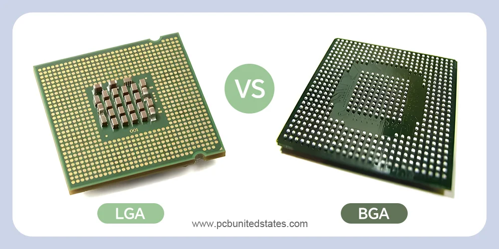
LGA (Land Grid Array)
The bottom of an LGA has neatly arranged flat metal pads that align with pads on the circuit board to establish electrical connections. Higher pin density and consequently better performance are made possible by this design.
- Pros: High pin density. Decreased risk of pin damage, Easy to inspect, Socket compatibility.
- Cons: Hard to align during installation, Limited heat dissipation.
- Ideal for: Modern processors, CPUs, Network controllers, FPGAs.
To better understand BGA vs LGA, take a look at: LGA vs BGA: Which Should You Choose?
CSP (Chip Scale Package)
CSP packages are typically no larger than the semiconductor chip itself, usually not exceeding 1.2 times the size of the corresponding semiconductor chip. This design maintains better electrical performance while enabling the installation of more chips in a smaller area. CSP IC package is ideal for compact, miniaturized devices.
Pros: Smaller size, Lighter weight, Enhanced electrical performance, Better thermal dissipation, Cost-effective.
Cons: High manufacturing cost, Limited thermal performance, Reliability concerns, Testing complexity.
Ideal for: Smartphones, Tablets, Wearable devices, Implantable and portable medical devices.
CSP common variants: WL-CSP (Wafer-Level CSP ), FC-CSP (Flip Chip CSP), LFCSP (Lead Frame CSP)
IC Package Recommendations For Common Scenarios
The table below provides recommended IC package types for common scenarios, along with key considerations behind each recommendation.
| Scenario | Recommended IC Package Types | Key Considerations |
| Prototyping | DIP, SOP | Easy to handle, ideal for manual soldering and breadboard testing. |
| Compact devices | QFN, CSP | Small footprint, supports device miniaturization. |
| High-speed or high-frequency circuits | BGA, LGA, QFN | Short interconnections reduce inductance and improve signal integrity. |
| High-power applications | QFN with exposed pad, BGA | Enhanced heat dissipation. |
| Consumer electronics | CSP, QFN, SOP | Compact size, supports miniaturization and mass production. |
| Automotive electronics | QFP, BGA | High reliability and resistance to temperature changes and vibration. |
| Industrial applications | DIP, QFP, BGA | Durability, reliability, longevity, easy to repair and replace. |
| Aerospace and defense | CSP, BGA, LGA | Lightweight, compact, extremely dependable in harsh circumstances. |
Conclusion
It’s critical to choose the right IC package. You’d better consider the key factors we discussed above before making your selection. Every project has different requirements. A package suitable for consumer electronics, such as smartphones, may not be suitable for industrial equipment or aerospace. You need to understand your project requirements completely and then choose accordingly. Don’t worry if you’re still confused. MOKOPCB is available to help. Our goal is to assist you in locating the best IC package for your requirements.
