PCB trace is a conductive pathway that connects components on the printed circuit board, allowing electrical signals, power, and ground between them.
Proper PCB trace design is fundamental for PCB operation. If we consider PCB traces as highways that connect cities, the design of the PCB width, length, and trace is as important as that of the highway. In this blog, we will systematically introduce you to how you should size and route PCB traces to ensure reliable performance, manufacturability, and efficiency for your projects.
What Should You Consider Before Sizing and Routing PCB Traces?
Before sizing and routing PCB traces, you need to carefully evaluate these 5 critical factors for greater electrical performance and manufacturability.
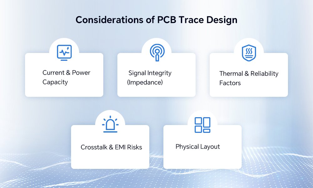
1. Current & Power Capacity
PCB traces must handle the required current without overheating or excessive voltage drop. A thicker or wider trace can carry more current, while long traces may need extra width to minimize resistance (IR drop).
Always check standards like IPC-2221 to determine the minimum width based on current, copper weight, and acceptable temperature rise. High-power traces, such as those for motors or power supplies, may require thicker copper (e.g., 2oz) or multiple layers to avoid overheating.
2. Signal Integrity (Impedance)
Signal integrity ensures high-frequency signals propagate without distortion or loss. Controlled impedance is crucial to reliable signal integrity. Impedance is the opposition to alternating current(AC) to high-frequency signals offered by the combined effect of resistance and reactance in a circuit.
Proper impedance matching can ensure consistent trace geometry so as to avoid signal reflection, EMI, and data corruption. Especially for high-speed signals (e.g., USB, HDMI, or memory buses), maintaining consistent trace impedance is extremely crucial to maintain clean and stable signals.
3. Thermal & Reliability Factors
Traces carrying high currents generate heat, and thin wiring may age or break due to continuous heating, leading to failure and thermal damage over time. Poor thermal design can accelerate aging or trigger thermal runaway in nearby components.
Wider traces, thermal relief pads, and copper pours help dissipate heat while avoiding long, thin traces reduces mechanical stress. In high-power designs, copper pours or delicate thermal relief structures are needed for safety and a longer lifespan.
4. Crosstalk & EMI Risks
Crosstalk refers to the unwanted coupling of signals between adjacent traces caused by parasitic capacitance and inductance, leading to signal distortion, noise, and mis-triggering. It is commonly seen in high-frequency, long-distance parallel or densely routed traces.
EMI(electromagnetic interference) originates from high-frequency signal radiation or circuit defects, which may be caused by high-speed signals, switching power supplies, or defective circuits (such as ground bounce). This may cause device non-compliance (such as FCC/CE certification failure), system misoperation, or interference with wireless communication.
5. Physical Layout
Narrow trace spacing may cause trace signals to interfere with each other, which may lead to data errors and signal distortion. In high-voltage applications, it may also lead to arcing or a short circuit. Keep proper trace spacing based on voltage levels, frequency to maintain the overall performance and reliability of electronic devices.
Proper Parameters for PCB Trace Sizing
To ensure reliable power delivery while optimizing PCB space, designers must carefully balance trace width, copper thickness, and trace length for fluent current flow and better thermal and electrical performance.
1. Trace width
The PCB trace width is one of the most important factors in PCB trace design in that it can directly affect the current-carrying capacity, heat dissipation, and signal integrity. If the trace is too narrow for the current flowing through it, the higher resistance of the trace will cause excessive heat, which may damage the traces.
The calculation of trace width has different standards, like IPC-2221 and IPC-2152, which are the two most commonly used standards. Here, we use the IPC-2221 formula to estimate the minimum trace width for a given current and allowable temperature rise:
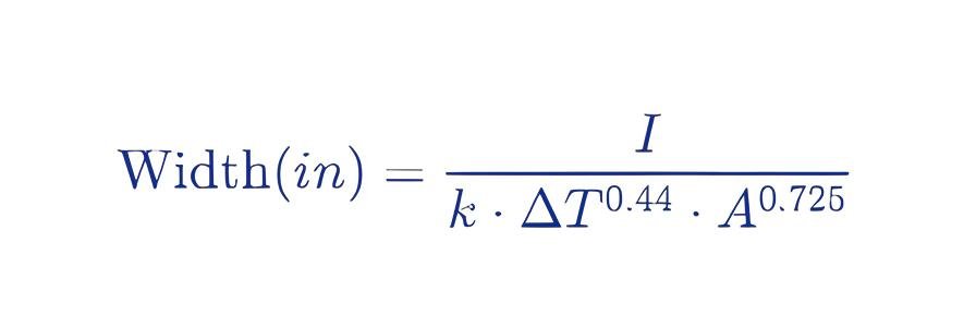 Where:
( I ) = Current (Amperes)
( ΔT ) = Temperature rise above ambient (°C, typically 10°C–30°C for safety)
( A ) = Cross-sectional area (mils², depends on copper thickness)
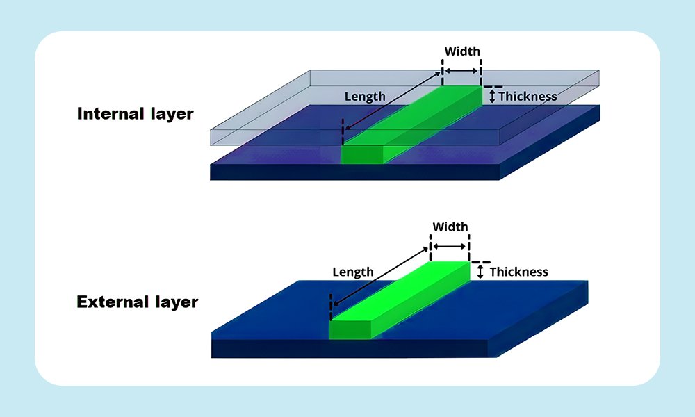
( k ) = Derating factor (0.024 for external traces, 0.048 for internal traces)
The external trace is the visible pathway, while the internal trace is the invisible pathway between layers.
Although there are also some typical trace widths in some PCB design tools and factories, these defaults are only feasible for ordinary low-current signals and are not always suitable for PCB traces. Most PCB designs use trace widths ranging between 6 mils (0.15 mm) and 100 mils (2.54 mm), depending on accurate parameters in different applications:
| Application | Typical Width (mils) | Key Consideration |
| Digital (Low-Speed) | 5–10 | Routing density |
| Digital (High-Speed) | 8–15 | Impedance matching, crosstalk |
| Power (Low-Current) | 15–30 | Voltage drop, IR loss |
| Power (High-Current) | 50–200+ | Heat dissipation, current capacity |
| RF & Analog | 10–20 | Controlled impedance, noise immunity |
| High Voltage | 30–50+ | Creepage clearance, arc prevention |
2. Thickness
Generally, copper thickness is adjusted according to different current or spatial requirements, for example, two can increase copper thickness in a limited space to keep current handling in narrower traces.
Thicker copper (e.g., 2 oz) supports higher currents and better heat dissipation but increases fabrication cost and etching difficulty, while thinner copper (e.g., 0.5 oz) is used for high-frequency/RF designs to minimize skin effect losses.
The calculation of the trace thickness is actually measured by the weight per square foot (oz/ft²) or microns (µm). Standard PCBs default to 1oz copper thickness, but it is also available in most PCB factories, varying from 0.5 oz/ft² to 3 oz/ft², with some options up to an uncommon 6 oz/ft². Here are common standards:
| Copper Weight (oz/ft²) | Thickness (mils) | Thickness (µm) | Usage |
| 0.5 oz | 0.7 mils | 17.5 µm | Ultra-thin (flex PCBs, high-density designs) |
| 1 oz | 1.37 mils | 35 µm | Most common (signal traces, standard PCBs) |
| 2 oz | 2.74 mils | 68 µm | High-current power traces |
| 3 oz+ | >4.1 mils | >105 µm | Extreme power handling (motor controllers, high-voltage PCBs) |
Note:
1 mil = 0.001 inch = 25.4 µm
1 oz/ft² ≈ 1.37 mils (35 µm) thickness
Outer layers typically use 1 oz or higher for durability and current handling, and inner layers often use 0.5 oz to 1 oz for a balance between fine traces and manufacturability. MOKOPCB supports custom trace thickness (0.5 oz – 5 oz+) for specialized applications. Contact us for more details.
3. Length
PCB trace length also affects signal integrity and timing in high-speed circuits. Typical trace lengths vary based on the application. However, short traces (a few millimeters) are preferred for avoiding issues like timing errors, propagation delays, and EMI(e.g., in DDR memory or USB data). Of course, longer traces (several centimeters) may be acceptable for low-speed signals such as power distribution or UART communication.
To minimize issues, critical traces should be length-matched and kept as short as possible to reduce parasitic inductance, resistance, and susceptibility to noise. PCB designers also always prioritize short and direct routing but avoid long traces.
Crucial rules for PCB trace routing
Effective PCB trace routing is the backbone of a high-performance circuit board. To ensure optimal functionality and manufacturability, adhere to the next 8 rules in PCB trace routing.
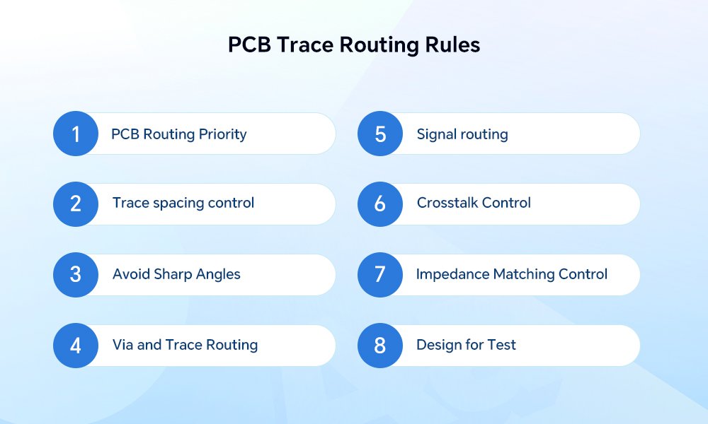
1. PCB Routing Priority
Critical Signal Priority. Critical signals such as power lines, analog small signals, high-speed signals, clock signals, and synchronization signals must be routed first. These signals directly impact circuit performance, and any interference or delay can cause system failure.
Prioritize routing the high-density areas. Start routing from components with the most complex connections or the densest wiring areas on the board. This ensures better organization and reduces congestion in critical zones.
2. Trace Spacing Control
Follow the 3W rule —— line spacing ≥ 3×line width. If the distance between the line centers is not less than 3 times the line width, 70% of the inter-line electric field can be maintained without interfering with each other.
For standard FR4 PCBs, maintain at least 0.1mm (4 mil) spacing between traces. High-density designs (e.g., HDI) may use 0.075mm (3 mil), but this increases cost and reduces yield.
3. Avoid Sharp Angles
Sharp angles (<90°) may retain etching chemicals and reflect high-frequency signals, causing copper corrosion or breaks, degraded signal integrity, and discontinuous impedance.
For general routing, obtuse angles (>90°) reduce etching defects like acid traps or copper cracks. For high-speed signals, use 45°bends or smooth curves for high-speed signals to maintain impedance consistency.
4. Via and Trace Routing
Proper via and trace design is essential for ensuring signal integrity and manufacturability in PCB layouts. Vias must be sized appropriately—high-current traces may need multiple vias, while high-speed signals avoid stub vias to reduce signal distortion.
Maintain a minimum clearance of ≥0.2mm (8 mil) for mechanical drilling processes and a spacing of ≥0.1mm (4 mil) for laser-drilled (HDI) vias to prevent manufacturing defects. Adding teardrops at via-trace junctions can also prevent cracking when designing.
5. Signal Routing
Critical signals like sensitive analog traces require dedicated routing layers to ensure their minimum loop area and reduce crosstalk and interference. If possible, you can take some measures like shielding and increasing the safety distance to minimize noise and maintain signal quality.
Moreover, matched trace length of critical signals is also important. Uneven trace lengths can introduce timing mismatches, resulting in errors or unreliable system performance. So, make sure the traces are as short and direct as possible for critical signals.
6. Crosstalk Control
Crosstalk is the mutual interference caused by long parallel wiring between different networks on a PCB, mainly due to the distributed capacitance and inductance between parallel lines. To avoid such a situation, you can:
1. Follow the 3W principle mentioned in point 2, “Trace spacing control”.
2. Insert grounding isolation wires between parallel lines.
3. Reduce the distance between the wiring layer and the ground plane.
4. Avoid routing different signal lines in the same direction on adjacent layers to reduce unnecessary interlayer interference.
7. Impedance Matching Control
Networks with impedance control requirements should be arranged on the impedance control layer to avoid signal cross-segmentation. Single-ended signals (like a 50Ω microstrip on FR4) must maintain 5%~10% tolerance, while differential pairs require tight spacing (≤2× line width) and length matching (±50 mil) for optimal performance.
To ensure signal integrity, avoid routing impedance-sensitive traces across plane splits or layer transitions. Instead, keep them on continuous reference planes (e.g., solid GND) and use impedance calculators (like Saturn PCB Toolkit) for precision design.
8. Design for Test
To enhance testability, ensure there are accessible test points(perfect in 1mm diameter) in critical signals for probing. Avoid placing test points under components like BGAs, as this complicates inspection and debugging. Additionally, automated optical inspection (AOI) requirements should be considered by maintaining ≥0.2mm (8 mil) line spacing for reliable detection.
Conclusion
As an important aspect of PCB layout, designing each PCB trace is crucial for the overall performance of the circuit board. Before designing a PCB trace, we need to consider some key factors that can influence PCB electrical performance and manufacturability, such as current capacity, impedance. It is also essential to figure out the important parameters and rules in sizing and routing the PCB trace to lay out an operational and reliable trace network.
MOKOPCB offers expert PCB trace design services with a professional team and superior quality. No matter whether you need custom trace widths, complex HDI routing, or thermal relief strategies, MOKO ensures high-quality PCB solutions for your specific requirements.
