PCB panelization is an important step in the circuit board production. A PCB panel combines many small printed circuit boards into one larger board. Compared to producing PCBs individually, panelization not only improves production efficiency but also allows for maximum output. Next, let’s learn more about how PCB panels drive efficiency in PCB production and everything you should know.
What Is a PCB Panel?
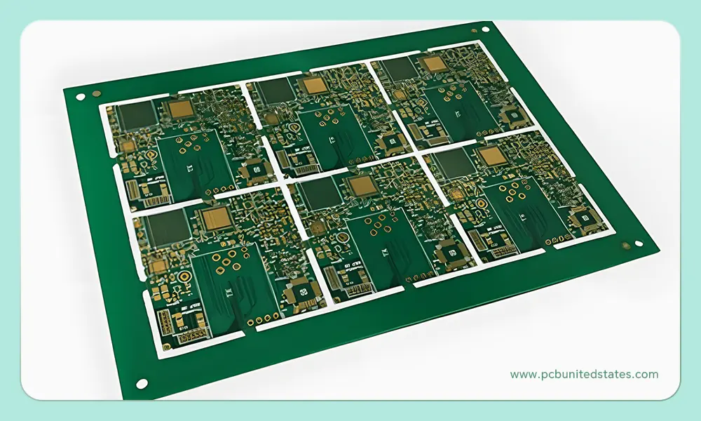
A PCB panel, also called a PCB array, is a larger circuit board that contains many individual boards combined, allowing for easy movement in the assembly line. The circuit board panel can have the same design or a different one. PCB panelization enables these small circuit boards to be manipulated at the same time, highly improving the efficiency.
Why Circuit Board Panels Are Critical?
Can you imagine that thousands of individual PCBs need to be handled and processed individually? How inefficient would that be? That’s why PCB panels play a vital role, improving the overall efficiency of the process. Let’s learn more benefits together.
Higher production efficiency: The boards are processed simultaneously, reducing the number of process steps. This can ensure a maximum output in a short period, which is critical for large-scale production.
Lower manufacturing costs: Shared initial setup and materials, minimizing waste and tooling expenses. For mass production, this can reduce unit PCB manufacturing costs.
Better assembly speed: The pick-and-place machines can place components on many boards in one run during the PCB assembly process, decreasing the process time.
Minimized damage risks: PCB panelization can protect the circuit boards from mechanical stress, vibration, and shock, avoiding damage during the manufacturing process. PCB panel is easier to assemble, transport, and store.
Consistent quality: All the individual PCBs in the large PCB panel undergo soldering and testing in the same conditions, following the standard procedures. Finally, this consistency improves high quality and minimizes the failure.
Different Types of PCB Panels
To accommodate different sizes and shapes of boards, there are various types of PCB panels to suit the circuit board design. Common types are as follows:
Standard Panelization for Simplicity (AAAA)
It is the most common kind of panel, featuring general compatibility. Identical PCBs are placed in a regular grid to form a panel. It simplifies designing, depanelization, and production planning, ideal for high-volume, uniform boards.
Rotated Panelization for Better Material Usage
This type of PCB panel is suitable for irregularly shaped PCB designs. Some PCBs can be rotated 90 or 180 degrees to maximize material utilization in a panel. But there are some disadvantages to this approach as well. It can lower the assembly speed. Due to the rotation, it is also difficult to inspect the circuit board, and the error rate of visual inspection increases.
Combination Panelization for Complex Designs (ABCD)
Combination panelization has various circuit boards with different designs, which are combined according to certain principles. It is ideal for toy electronics and home compliance, requiring different types of PCBs. But on the assembly line, managing product variations is a challenge. If one board in the panel fails quality inspection, it affects the overall yield. The panel cannot deliver a full set of boards.
3 Main PCB Depanelization Methods
These days, there are three main techniques for PCB panelization, and each has advantages and disadvantages. Often, the PCB design determines which one to utilize.
V-Scoring
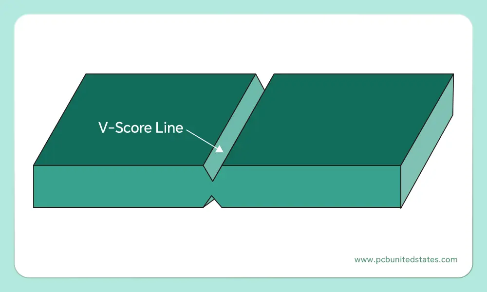
Use an angled blade to remove one-third of the thickness along the top and bottom of the PCBs, creating a straight V-shaped score line between the individual circuit boards. The remaining one-third of the thickness of the material holds the boards together. After assembly, tools are generally used to separate them along the V-groove.
Pros: This is a fast and cost-effective solution, ideal for straight-line separations.
Cons: It is only ideal for rectangular or straight-edged PCB designs and can leave rough edges if not done precisely. If the components are hung on the PCB edge, they may be damaged when separating.
Tab Routing
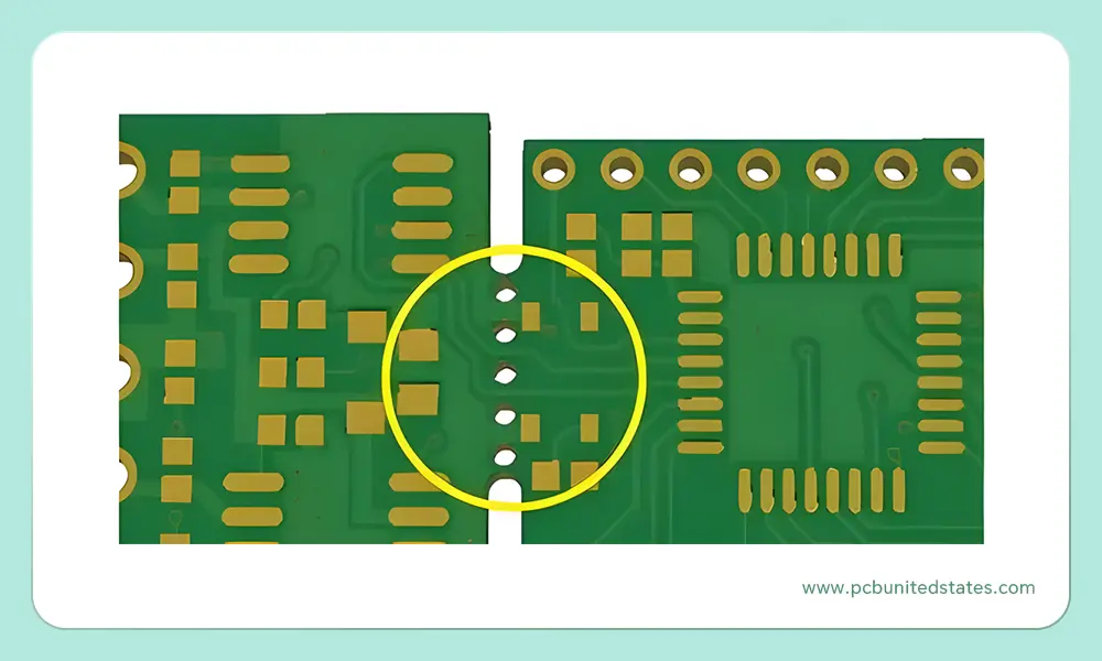
When V-scoring is not suitable, tab routing is used instead. When using tab routing, the PCB is pre-cut and then connected using small tabs (mouse bites) with perforations, typically 3 to 5 holes. PCB designs with components that hang over the edge can be supported by this technique.
Pros: It’s suitable for complex shapes and non-rectangular PCB designs. The boards can break out from the PCB panel by hand with better edge quality than V-scoring.
Cons: It requires previous cutting steps, making it slower than V-scoring. There may be some small bumps left that will need to be sanded down.
Solid Tab Routing
Solid tab routing is similar to tab routing, but without perforations. PCB boards are connected by solid tabs. When depaneling, the PCB panel must be cut using tools.
Pros: It offers strong panel rigidity during the assembly process, minimizing movement.
Cons: This method requires additional cutting steps, featuring low efficiency.
V-Score Panelization vs. Tab Routing Panelization
When choosing V-Score panelization vs. tab routing panelization, it highly depends on your PCB design. The table below highlights their 8 differences to help you make the right choice.
| Aspects | V-Score Panelization | Tab Routing Panelization |
| Connection | V-shaped grooves | Small tabs |
| Separation Method | Separate along the score lines | Break tabs manually or with tools |
| PCB Shape Compatibility | Rectangular or square-shaped PCBs | Odd-shaped PCBs |
| Edge Quality | Rougher edges, may need light sanding | Smoother edges, but small bumps may remain |
| Speed | Very fast | Slower than V-scoring due to extra routing time |
| Cost | Lower cost | Slightly higher cost |
| Edge Components | Not ideal for components near edges | Works well with components near edges |
Best Practices for PCB Panel Design
Using Pallet Rails for Panel Support
It’s important to use removable rails for additional support. These are thin strips of material, typically 5-8 mm wide, added to the edge of the PCB panel. The rails can be easily removed after assembly and testing, leaving smooth and clean edges.
Adding Fiducials for Accurate Alignment
Fiducials are small reference points on a PCB that serve as alignment targets for automated equipment. They can be divided into global fiducial markers (on board edges for orientation) and local fiducial markers (near components for footprint recognition).
– The ideal diameter ranges from 1 to 3 mm.
– Keep at least 3 mm clearance from the board edge.
– Place three global fiducials on the edge of the PCB.
– For SMT components, place at least two local fiducials diagonally on the outside.
Incorporating Tooling Holes for Efficient Handling
The PCB panel needs to remain stationary during the drilling and assembly process. To make it easier for the machine to push the panel for alignment, the tool holes are positioned on the panel’s edge. These holes don’t have a set size., and they can be determined based on actual conditions.
V-Groove Design Guidelines
In the cutting process, the components should maintain a proper clearance of 0.05 inches with V-grooves. For taller components like ceramic chip capacitors, the clearance should be at least 1/8 inch.
V-grooves can reduce structural integrity, causing leading and trailing edges to sag during wave soldering. Finally, the PCB panel can warp or jam in the machine. Jump-scoring can be used to strengthen PCB arrays and avoid these problems.
Optimizing Breakout Tab Placement
The components should keep at least 0.125 inches away from the tabs. For taller components, the distance should be 0.250 inches. The copper trace needs to be 0.125 inches away from the tab to avoid interference from the cutting tool.
Final Words
PCB panel design is a crucial and complex process that directly affects the success and cost of your project. Among them, the choice of PCB depanelization method is especially important. With rich experience, MOKOPCB can provide professional PCB panel design services to help you achieve success. Contact us to start your next PCB project!
PCB Panels FAQs
- What are the standard sizes of PCB panels?
These are common standard panel sizes: 18 inches × 24 inches, 18 inches × 12 inches, 9 inches × 12 inches, 9 inches × 24 inches.
- Can I customize the PCB panel size?
Of course! You can customize the panel size to suit your PCB design, but there’s a balance to be struck between customization and manufacturability. This is exactly where MOKOPCB can help you.
- When should panels be used?
PCB panels are useful in situations such as:
– The PCB is too small for automated equipment to handle.
– PCB production is in large quantities, and PCB panels can improve efficiency and save costs.
-The components are too close to the edge, and the panel has guide rails, which makes it safer during assembly.
- What factors need to be considered when PCB paneling?
The most noteworthy factors include: PCB design, components, materials, etc. All these factors impact the choice of paneling method and limit the available solutions.
