Whether it is a simple or complex board, a good PCB design ensures that the circuit board will function as intended and can be manufactured in volume. In this blog, we’ve compiled 10 PCB design guidelines that apply to most standard circuit boards. These rules cover key aspects, including manufacturability, stackup arrangement, component placement, thermal management, etc. Helping designers create high-performance and high-reliability PCBs in 2025.
Rule 1: Ensure Manufacturability in PCB Design
When it comes to the PCB design guidelines, manufacturability is the first critical consideration. Even though a design is perfect, it cannot be considered a truly successful result if it is difficult to produce. The designers should take into account factors like the capabilities of manufacturing equipment, the availability of materials, and the ease of assembly.
Rule 2: Strategic Plan PCB Stack Up
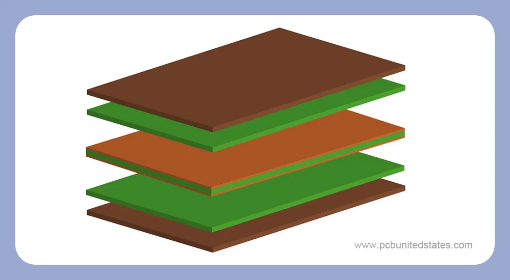
One important rule in PCB design guidelines is to strategically plan the PCB stackup. Each layer has its specific function. The arrangement of these layers affects not only aesthetics but also performance. A well-planned stack-up can minimize EMI (electromagnetic interference) and maintain signal integrity.
The key to achieving signal integrity is preserving the shape and timing of the signal. This can be achieved through carefully designed stacking to minimize signal loss and crosstalk. Besides, electromagnetic interference can cause damage to your circuits. However, a well-designed stack-up can help control EMI by providing shielding and current return paths.
Rule 3: Separate Analog and Digital Blocks
Sometimes, analog and digital signals may need to run on the same circuit board. If these signals are mixed, they share the same current return path. Noise from the digital circuits may interfere with the analog circuits, causing signal distortion and performance degradation. By properly partitioning analog and digital modules in the layout, you can ensure circuit stability and reliability. Here are some useful practices:
- Place sensitive components (voltage reference and amplifiers)on the analog plane. Likewise, position noisy components (timing blocks and logic control) on the digital plane.
- One mixed-signal ADC(analog-to-digital converter) or low digital current DAC (digital-to-analog converter) can be placed in the analog plane. For multiple high-current ADCs/DACs, it is advised to separate the digital and analog power supplies.
- Microcontrollers and microprocessors should be placed close to related modules as well asin the center of the PCB to facilitate heat dissipation and routing.
Rule 4: Plan Component Placement Wisely
Component placement directly impacts circuit performance, manufacturability, and accessibility. In this process, you may face different challenges and have to consider many PCB design guidelines. The following are some crucial rules:
- Put the critical and necessary components first, then other parts, to avoid mechanical enclosure or size limitations.
- For high-speed, analog, and power circuits, it’s recommended to place the components closely to keep short and direct traces.
- For large ICs and processors, it’s advised to put them centrally to simplify trace routing.
- Place all the SMD components on the same side to simplify assembly and reduce costs.
- To ensure manufacturability, avoid placing components too close together to prevent automated assembly.
- Accessibility is also critical. The components should be easy to access for testing, rework, etc.
Rule 5: Design for Effective Thermal Management
An effective thermal management design can ensure components’ reliability and extend their lifespan. Some PCB design guidelines for heat dissipation are as follows:
Thermal vias: They offer an efficient thermal path from components to the surrounding PCB material.
Heat sinks: They are installed on high-power components to lower their operating temperature and avoid overheating.
Copper pours:It’s effective to dissipate heat more evenly by using large copper pours on the power layer and ground layer.
High thermal conductivitymaterials: To aid in heat dissipation, you can also use PCB materials with excellent thermal conductivity, including ceramic substrates or aluminum.
Rule 6: Optimize Trace Routing to Maintain Signal Integrity
Thoughtful trace routing is essential for reliable PCB performance and high signal quality. Here are the key PCB design guidelines that you should keep in mind:
Trace length: Keep traces as short and direct as you can to minimize the crosstalk and maintain the proper spacing.
Trace width: Keep routing width consistent within the same network to maintain uniform impedance and minimize reflections.
Routing angles: It’s highly recommended to use smooth 135-degree bends, not right angles or sharp angles in traces, as they can radiate noise and degrade performance.
Return paths: Ensure clear and short return paths for signals on reference planes to maintain signal integrity.
Orthogonal routing: In order to minimize crosstalk, route traces on adjacent layers in orthogonal directions.
Rule 7: Arrange Power and Ground Planes Properly
Power and ground planes are commonly arranged on the internal layers, keeping them symmetrical and centered. For PCBs with at least 4 layers, use a complete ground plane rather than a separate ground trace. With components that require a direct power connection, a shared power rail can be used if a dedicated power plane is not available. However, avoid daisy-chaining power supplies. Besides, it’s important to ensure the traces are wide enough. Narrow traces can heat up or even burn out when high current flows.
Rule 8: Optimize PCB Panel Layout for Production
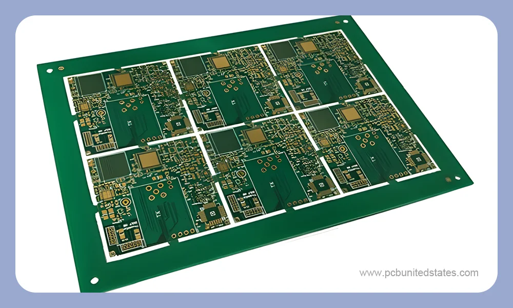
In circuit board design, properly optimizing PCB panel layout can help reduce manufacturing costs and improve production efficiency. Contact the PCB manufacturer to obtain their recommended panel dimensions, then adjust your design accordingly. You should apply a layout that fits the preferred panel sizes of the manufacturer, repeating the design whenever possible.
Rule 9: Leverage Screen Printing for Efficiency
Silkscreen printing is used to mark various information on circuit boards, playing a vital role in assembly and maintenance. A clear and well-designed silkscreen design can indicate component position, polarity, orientation, test point indicators, manufacturer information, board version, etc. It helps assemblers quickly locate components, efficiently completing installation and soldering. Also, silkscreen printing can facilitate subsequent debugging and repairs. It’s important to note that the silkscreen should avoid covering solder pads and remain clear and easy to read.
Rule 10: Perform Checks Regularly
Before moving to production, you’d better verify the design regularly and repeatedly. Any errors can impact the later production and assembly. We recommend that you always perform DRC and ERC in the design process to verify that your design is correct. It only takes a little time to run DRC, which can significantly save time on later debugging and changing. Moreover, continuous checking is a good habit worth maintaining.
Conclusion
By learning these top 10 PCB design guidelines, designers and engineers can streamline the design process, acquiring reliable and high-performance circuit boards. In actual practice, these rules can ensure smooth manufacturing and stable performance. However, for some special and complex circuit boards, we also need to follow additional and special PCB design guidelines to meet performance and reliability requirements.
