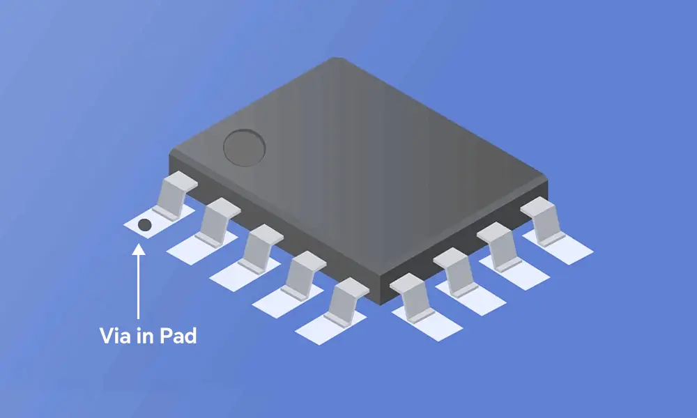
Nowadays, engineers and designers often face the demand for higher component density, faster signals, and compact PCB layouts. Via in pad PCB can satisfy these requirements. The via is directly placed under the pad of SMT components. It can simplify routing as well as achieve connections between components and internal layers. When choosing via in pad PCB design, you can acquire a smaller component pitch, reducing the overall board size. Do you know when to use via in pad PCB design? Or is it even necessary? By reading this article, you will clear up all the confusion and get what you desire.
When to Use Via in Pad PCB Design?
Below are the main situations where via in pad PCB design is especially beneficial:
When Handling High-Density Layouts
When designing an HDI PCB, the components need to be mounted within a limited board space. At the same time, high-density wiring is also required. The via in pad PCB design can reduce the number of vias on the board, saving space and enabling higher component density. This technology is particularly important for miniaturized electronic devices such as IoT devices, smartphones, and wearables.
When Better Thermal Management Is Needed
Via in pad PCB also acts as a thermal via, offering a direct thermal path from components to the internal copper plane. It can effectively dissipate the accumulated heat from temperature-sensitive or high-power components, such as power amplifiers, high-power LEDs, and voltage regulators. The risk of overheating can be greatly reduced, thus enhancing the reliability of the components under usage.
When Working with Fine-Pitch Components
Via in pad PCB is frequently used in BGA (Ball Grid Array) and QFN (Quad Flat No-Leads) packages, which have high-density IO (input and output) connections under the chip. For BAG chips, there are a larger number of pins and the spacing is close, bringing a challenge for tracing. When using this via, it is easy and quick to transmit the signals from components to the inner PCB layers. For QFNs, it’s an effective solution to optimize routing and thermal management.
When Optimizing Signal Integrity
Signal integrity is important in high-speed and high-frequency circuits. Via in pad PCB allows signals to be passed directly from the components to the inner layers, significantly shortening the PCB trace path. This design reduces parasitic inductance and capacitance, as well as improves impedance stability, ultimately enhancing the signal integrity.
When Standard Vias Are Enough
If you have sufficient PCB space, traditional vias placed near the pad can meet the design requirements. These options are simpler and often more cost-effective compared to via in pad PCB design.
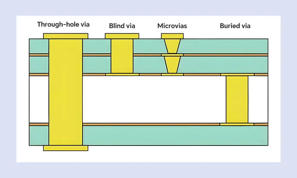
Through-hole via
It’s a common type of via that is drilled through from the top to the bottom, linking all PCB layers. With a simple structure, these vias are easy to drill and are cost-effective, but they occupy more space on the board.
Blind via
It doesn’t go through the whole PCB, only connecting the outer layer to one or more inner PCB layers. You can just see the via on one side of the PCB, so it is called a blind via. Compared with a through-hole via, a blind via is hard to manufacture, but it can save board space.
Buried via
It is used to link the adjacent inner layers of PCB, and can not be seen outside of the circuit board. This via type is used for at least 4-layer PCBs. Compared to blind vias, buried vias are more complicated and costly to produce.
Microvias
These are very small holes that require a laser to drill and are commonly used in HDI PCBs. Their hole diameter typically is less than or equal to 6 mils. Microvia can connect adjacent layers or multiple layers in a stack-up.
Below is a simple table to help you better distinguish these vias, highlighting when standard vias may be sufficient vs. when via in pad PCB becomes necessary.
| Via Type | Layer Connection | Fabrication Difficulty | Space Requirement | Drilling Method | Cost | Typical Application |
| Through-hole via | Top → Bottom | Easy | High | Mechanical drill | Low | Standard multilayer PCBs |
| Blind via | Surface → Inner | Moderate | Medium | Mechanical drill | Medium | Space-saving in compact designs |
| Buried via | Inner → Inner | Hard | Low | Mechanical drill | High | High-layer-count PCBs |
| Microvia | Surface → Inner | Hard, laser | Very low | Laser drill | High | HDI designs, smartphones, wearables |
| Via in pad PCB | Surface → Inner | Very hard (filled & capped) | Minimal | Laser drill + fill & cap | Very high | Fine-pitch BGA/QFN, thermal vias |
As the table shows, standard vias are easier and cheaper to manufacture but take up more space. While via in pad PCB can achieve high-density design and better performance at the cost of greater complexity.
Why Via in Pad PCB Is Not Always the Best Choice
Although via in pad PCB is very useful in high-density designs, it has certain challenges. Such issues, when not properly handled, can affect the reliability of the electronic device. These challenges explain why via in pad PCB design should be used only in specific scenarios.
Increased Manufacturing Complexity
Via in pad PCB routing requires additional steps, highly increasing manufacturing complexity. Manufacturers need to drill additional vias, plate them with conductive materials, then fill them with epoxy, and cap them with copper.
Risk of Outgassing
With the soldering process, the capped vias are likely to outgas. This is caused by heating, which causes the liquid to turn into vapor. Air bubbles travel upwards through the via-in-pad, and such outgassing may result in voids in the solder joint.
Surface Planarity Issues
The surface bumps can be a result of an imperfect filling and covering of the via in pad PCB. These bumps bring a challenge to component soldering, mainly the BGAs. It is essential to keep the surface flat, as this will affect the PCB assembly.
Design Constraints
When designing via in pad PCB, you need to be mindful of their effect in subsequent assembly. If the vias are not properly filled and capped, there is a risk of solder entering the vias in the soldering process. Finally, it may cause weak solder joints.
Impact on Electrical Performance
As well as contributing to better routing density and signal integrity, via in pad PCB can contribute to worse problems when misused. Solder joint defects can cause signal degradation or impedance changes. These problems may have implications for the electrical performance and even cause failure.
Best Practices for Using Via in Pad PCB Design
Once you’ve determined that via in pad PCB is the right choice for your design, the following practices can help you implement it successfully. By following proven practices, it’s easy to reduce risks and avoid costly mistakes during PCB assembly.
Assess PCB Manufacturer’s Capabilities Early
Before you begin designing your circuit board, evaluate your PCB manufacturer’s design and manufacturing capabilities, such as the minimal annular ring size. This will avoid DRC and DFM issues later on.
Verify Exported Design Files
When exporting from the PCB design software, it’s critical to review all design files. This can avoid many errors and issues that may occur during later fabrication. In addition to the standard drill diagram, a separate file that highlights only the via-in-pads is crucial. These files can help manufacturers clearly distinguish them from traditional vias, preventing them from mistakenly cap or fill.
Control Materials and Process to Avoid Surface Bumps
To ensure a smooth soldering process, you can select suitable materials and maintain strict process control to prevent surface bumps. It includes a carefully controlled fill and cap step to provide a smooth and even surface for reliable component placement.
Sizing Rules for Via in Pad PCB Design
For dependable connections, the pad size should typically be a little larger than the via size. When designing the hole size of the via in pad PCB, it’s advised to add a suitable tolerance for accurate drilling. It’s necessary to maintain an adequate annular ring around the via, which can impact PCB electrical performance.
Test and Inspect Before Mass Production
Before moving to large-scale production, it’s necessary to test whether the via in pad PCB design meets the required performance and reliability. Here are some key tests: solderability test, thermal test, and electrical testing. All these tests can guarantee the design is accurate to meet its intended function and ready for mass production.
Last Words
Learning from this blog, you’ve known when to use via in pad PCB design. It saves board space and increases routing density, driving the development of compact and wearable devices. Although via in pad PCB brings additional manufacturing challenges, it can be successfully implemented through careful design and collaboration with an experienced manufacturer. With nearly 20 years of industry experience, MOKOPCB provides one-stop PCB & PCBA services, including expertise in via in pad PCB solutions. Contact us to learn how we can support your next design.
