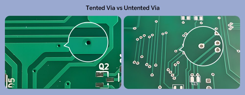
Via holes, one of the important PCB holes in PCB design, require appropriate protection when exposed to air. Effective protection ensures assembly reliability, extends the lifespan, and provides smooth surfaces. Via tenting is one of the most effective ways of covering to protect the opening via and the annular ring with the solder mask. Via tenting prevails for its effective via protection and cost-effectiveness, and let’s look into when to use via tenting in PCB design and how to use it wisely.
When to Use Tented Vias? ( 5 Major Purposes)
The main purpose of via tenting is to protect the vias from environmental factors, reduce accidental short-circuiting, and contact with the circuit. Here are 5 major purposes for tented vias.
Electrical isolation between nearby pads
By covering the solder mask on vias, tenting forms a barrier between the vias and surrounding conductive components, preventing electrical contact and accidental short circuits.
Prevent solder wicking and bridging
Solder masked barrier on the via prevents solder wicking in that solder from being draw into the via during reflow. Tenting covers the via to keep solder where it belongs. Besides, tented vias also prevent bridging by isolating unintended solder pathways between close vias and components. This precludes the possibility of short circuits, malfunctioning, and even expensive rework.
Avoid Oxidation and corrosion
Cooper within open vias is exposed to air and moisture, and is prone to being corroded and oxidized. Protective tenting ensures a longer lifespan and higher reliability. Especially for small vias less than 12 mil, protection has a better effect. If the via diameter is too large, the solder mask easily breaks and leaves a small hole, which may contaminate the vias.
Flat PCB surfaces for solder mask alignment and assembly
Open vias show as tiny holes on the PCB board, which may influence solder mask alignment and component placement. Tented vias with a flat surface enhance aesthetics and reduce assembly defects, like flux residue.
Balance cost and protection
Tenting is the simplest process that can be used to protect vias with the smallest cost compared to other via protection methods. It is a “good enough: solution when you have limited budgets.
Tips: When not recommended
When vias are used as testing points, vias should remain open to ensure test pins can make contact.
If the via serves as a thermal relief, keeping the via open is a must to improve heat dissipation efficiency.
When the via is under SMT pads(via-in-pad), simple tenting is not enough. Solder can still sink into the via and cause voids and poor connections. Try via plugging and via filling to ensure flat and solderable surfaces.
Choose Which Type of Via Tenting? (4 Types)
IPC-4761 defines 7 types of via protection methods. Among them, two major types(I and Type II) are related via tenting. Here are 4 types of via tenting: I-a, I-b, II-a, II-b.
Type I-a(One side via tenting): A basic form of via tenting that covers the via hole and its annular ring with solder mask on only one side of the PCB. It can provide basic protection, but may have long-term reliability issues.
Type I-b(Two sides via tenting): Both two sides of the via hole and the annular ring are covered with solder mask. This offers greater protection against oxidation, contamination, molten solder wicking, and solder bridging, providing a great balance between reliability and cost.
Type II-a(One side via tenting + covering): The via is tented on one side with solder mask and then reinforced with a second layer of solder mask on the via surface. It improves the sealing of via and minimizes the risk of mask cracking and pinholes.
Type II-b(Two sides via tenting + covering): This type of via tenting provides the robustest protection as both two sides of the via are sealed with solder mask. It ensures high reliability but costs more.
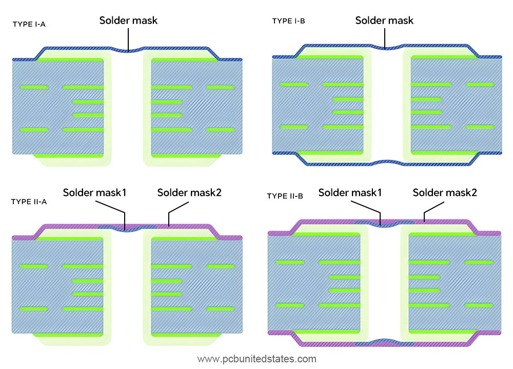
What’s more, the solder mask materials are also related to the selection of via tenting types. Generally, solder resist ink is cheaper and usually used for I-a and I-b via tenting type, while dry film solder mask is stronger and thicker to decrease the risk of pinholes and cracks, making it ideal for II-a, II-b types.
In practice, type I vias are the most common for their cost-effectiveness and simplicity. Type II is a better choice if your PCB pursues long-term protection and reliability.
Go beyond Via Tenting: Via Plugging and Via Filling
Only covering non-conductive solder mask on the via surface with an empty via barrel, via tenting saves much cost and is much easier to achieve. However, the mask may crack or blow out in harsh environments. So, have a look at the other 2 via covering methods for greater via protection and reliability, they are via plugging and via filling.
Via plugging is the process that partially seals one or two sides of vias with non-conductive or conductive materials, like epoxy resin or conductive paste, and the surface. The most common and widely used type is non-conductive via plugging, used to prevent the solder mask from flowing and contaminant storage. Conductive plugging is less common and is used for those who need thermal or electrical conduction, but it also comes with problems of faster metal expansion and possible fracture.
Via filling is to fill the whole via hole with conductive or non-conductive material, like copper and resin, and then plate over the via to make it flat. It can thoroughly eliminate contamination and solder wicking. Conductive materials can also establish an electrical connection between different layers.
Via plugging and filling delivers more advanced protection than tenting, for the vias are fully blocked with materials. This means that they can provide higher mechanical reliability and performance, but also come at a higher cost. They can play a better role in dense HDI PCBs, via-in-pad, thermal performance required applications.
| Method | Conductive | Cost | Protection Level | Common Use Case | Reliability |
| Tenting | No | Low | Medium – surface sealed | General signal vias | Basic |
| Plugging | Usually Non-conductive (can be conductive) | Medium | High – via barrel partially blocked | Prevent solder wicking, HDI | Medium |
| Filling | Yes (copper) / No (resin) | High | Very High – via completely sealed and flat | Via-in-pad, thermal vias, BGA | High |
Use via tenting wisely
Via tenting stands out as a practical and cost-effective via protection method in PCB design. It basically prevents solder wicking, oxidation, and electrical interference, balancing cost with protection. 4 types of via tenting(I-a, I-b, II-a, II-b) provide different levels of covering reliability, durability, and cost. At the same time, via tenting is not always the best choice in some situations, like via-in-pad design, and you may consider alternative methods such as via filling or plugging.
For projects where precision and high quality are essential, MOKOPCB provides professional PCB manufacturing with reliable via tenting solutions and other advanced via protection processes. Contact us freely, and we will help your PCB design and manufacturing achieve high performance and durability.
