Flying Probe Testing
With PCB designs becoming smaller and more complex than ever, it has never been more important to ensure that boards are manufactured defect-free straight out of the factory. The Flying Probe Test (FPT) is one of the most frequently used PCB testing systems, largely due to its versatility and cost-effectiveness.
This article explains how a Flying Probe Test works and provides practical information to help you decide when and how to apply it.
What Is a Flying Probe Testing?
Flying probe testing is an automated PCB testing procedure that checks the electrical functionality and integrity of the print circuit boards by using moving test probes. Unlike conventional in-circuit testing, which uses specific fixtures, flying probe machines use several probes that move freely across the board to test different points. There is no need to have costly tooling or setup time, making it an ideal choice for prototypes, low-volume production, and boards that change the design frequently.
How Does Flying Probe Testing Work?
The flying probe PCB test process for a PCB involves the following key stages:
Step 1: Preparing the Test Program
Prior to the procedure, the specialized software develops a program that assigns the probes where to move to and what to measure. This program is built using the design files of the board (like the ODB++ or IPC-2581) and the bill of materials. When finished, the program is uploaded into the tester, and the PCB or panel of boards loaded onto a conveyor system which carries the boards into the test chamber.
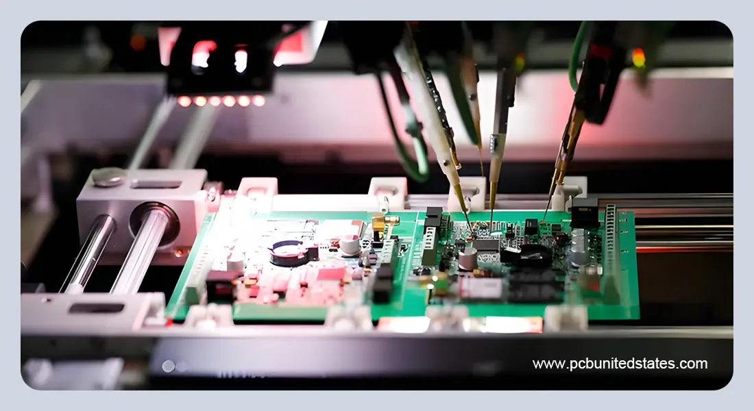
Step 2: Probes in Action
A set of probes moves freely within the tester board controlled by a computer. These probes contact one or more access points including:
- Component pads
- Dedicated test pads
- Open vias without solder mask
At every point, the system provides a stimulation or power with electricity and records a response of the board. This allows the tester to ensure that connections are in the right place, and components are working as desired.
Step 3: Measuring and Evaluating
The signals obtained are compared to the expected performance as set out by the design information. To carry out these tests, the tester operates sophisticated equipment such as power supplies, signal generators, multimeters and sensors.
One of the key features of this system is virtual isolation, which allows the tester to isolate certain circuit components electronically. Therefore, the individual component values can be accurately measured without removing them off the board.
Step 4: Final Assessment
Based on the entire measurements, the tester concludes on whether PCB is functioning well and electrically. Although probe access may limit complete coverage on some designs, flying probe systems remain a very useful means to discover defects in a prototype and low- to medium-volume production.
Components of Flying Probe Testing Systems
A flying probe test machine consists of three main components that work together to ensure accurate PCB testing:
- Probes
Probes are the contact interface between the tester and the PCB. Moved freely in the X, Y and Z directions,they access pads, vias, and other test points to transmit signals and to receive responses. There are 3 types of probes that are commonly used to meet particular requirements:
Spring-loaded probes: low-cost and very popular for standard testing.
Active probes: have onboard electronics that are used in high-frequency measurements or sensitive measurements.
Kelvin probes: use four wire technique for precise low resistance evaluation.
- Test Fixtures
The fixtures are used to hold the PCB in place during testing to ensure the stability and steady contact with the probes. The most typical are the so-called mechanical or universal fixtures, which are characterized by hard frame, clamps, and support pins. They are cheap and versatile but manual adjustment is usually required.
- Control Software
The software handles all the testing procedure. Its main tasks are to create test programs based on CAD formats such as ODB++ or IPC-2581 as well as to optimize probe routes to minimize cycle time, analyze the data collected and generate pass/fail reports with SPC charts. It is also able to integrate with AOI, X-ray or pick-and-place systems as well as having a user interface to monitor, log error and debug.
Types of Flying Probe Test Systems
A number of flying probe tester systems are fitted to meet particular testing needs and uses. There are primarily four kinds of flying probe test systems, including Single-sided Systems, Double-sided Systems, Vertical Systems, and High-speed Systems. A comparison of these types of systems is given in the table that follows:
| System Type | Brief Explanation | Typical Applications | Key Advantages | Key Limitations |
|---|---|---|---|---|
| Single-Sided | Probes access only one side of the PCB at a time, making it ideal for simpler, low-layer boards. | • Simple PCBs or PWBs • Low-volume or prototype testing • Boards with test points on one side only |
• Lower cost and compact setup • Good for continuity, shorts, and open-circuit checks • Ideal for single-sided PWB solder verification |
• Cannot access both sides simultaneously • Not suitable for dense or multilayer designs • Slower for complex circuits |
| Double-Sided | Probes contact both sides simultaneously, enabling faster and more comprehensive testing of complex boards. | • Complex or multilayer PCBs • Boards with test points on both sides |
• Faster and more accurate than single-sided • Handles high-density, high-layer designs |
• Higher equipment cost • Larger machine footprint • More maintenance complexity |
| Vertical | PCB is tested upright, saving floor space and easing handling of large or heavy boards. | • Large or heavy PCBs • Facilities with limited floor space • Lines needing upright handling |
• Space-saving vertical orientation • Easier handling of oversized boards • Can be single or double-sided |
• May require special fixturing • Operator training for vertical loading • Speed depends on configuration |
| High-Speed | Uses advanced motion control and precision probes to deliver rapid testing without sacrificing accuracy. | • High-volume production • Tight schedules requiring rapid throughput • Boards needing fast continuity and functional checks |
• Dramatically reduces test time • Maintains accuracy at high speeds • Maximizes production efficiency |
• Higher capital investment • Requires skilled calibration • Needs optimized test programs |
Flying Probe Test vs. In-Circuit Test (ICT)
Flying Probe PCB Test is frequently compared to In-Circuit Test (ICT), another common structural test used by engineers. The two methods test electrical performance, although their strengths vary.
| Feature | Flying Probe Test | In-Circuit Test |
|---|---|---|
| Setup Cost | No fixture required | Custom fixture required (high upfront cost) |
| Program Time | Hours | Days to weeks |
| Throughput | Slower per board | High speed, ideal for mass production |
| Flexibility | Excellent for design changes | Poor — new fixture needed for each revision |
ICT provides unbeatable speed with stable and high volume products and FPT offers maximum flexibility and low start up cost for prototypes, pilot runs and frequent engineering change. Large numbers of manufacturers employ both- they use Flying Probe Testing during development and then ICT when volumes justify the investment.
Benefits and Limitations of Flying Probe PCB Testing
Key Benefits:
- No fixture costs: In flying probe test, there is no need to use fixtures and other tools, which can reduce the upfront investment.
- Fast programming: The design of new boards can be tested in hours after receiving the design files.
- High accuracy: Modern FPT systems can identify even minor defects with high accuracy.
- Flexible and adaptable: This PCB testing technique can be easily adapted to design changes without using new fixtures, and is suitable for different board types.
- Both-sided testing: Tests both sides of the PCB simultaneously, boosting efficiency and accuracy without manual flipping.
Limitations:
- Reduced throughput: Flying probe testing performs measurements sequentially rather than in parallel, and therefore, it takes more time to run than ICT, especially when testing a board with many test points.
- Limited functional testing: It primarily tests the basic electrical parameters such as continuity, resistance and capacitance. It has a limited capability with complex powered functional tests.
- Probe access requirements: Dense component placement or limited test pads can restrict probe contact, potentially reducing test coverage.
Partner with MOKOPCB to Improve Your PCB Quality
At MOKOPCB, we understand the importance of detecting defects in the early stages of a project. Our Shenzhen plant is equipped with advanced Flying Probe Test systems that can test complex multilayer boards, fine-pitch components, and fast engineering changes. Our team can create test programs based on your CAD data and provide comprehensive reports that meet international quality standards.
We also utilize other complementary PCB testing techniques such as Automated Optical Inspection(AOI), X-ray inspection, and functional testing to ensure high reliability with fast turnaround times for our customers
Contact Us
Got any questions or inquiries? Fill out the form and we will get back to you soon