In-Circuit Testing
In-circuit testing(ICT) is one of the most commonly used PCB testing methods. ICT identifies defects early, minimizes scrap rates and keeps manufacturing standards by testing individual components and also by testing the connection in the production process. The following guide will discuss what ICT is, how it works, flaws it detects, and its advantages and disadvantages. Let’s dive right in.
What Is In-Circuit Testing (ICT)?
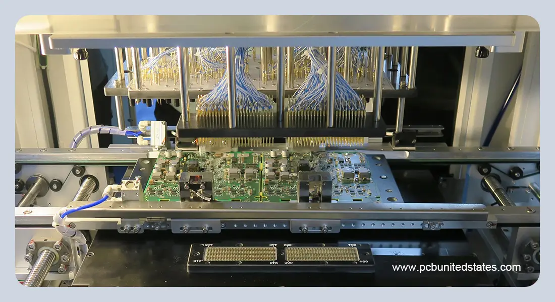
ICT is a testing method that uses a bed-of-nails fixture or test probes to make electrical contact with the specific points in the circuit boards. The in circuit test machine input controlled signals and measure parameters like resistance, capacitance, inductance, shorts, and opens to verify if the components are correctly placed and soldered. By identifying the assembly and manufacturing issues early, ICT ensures that each PCB can meet the expected performance before moving to the next production phase.
Key Elements of ICT Systems
There are some fundamental components of in-circuit testing (ICT), which work together to deliver precise and reliable results:
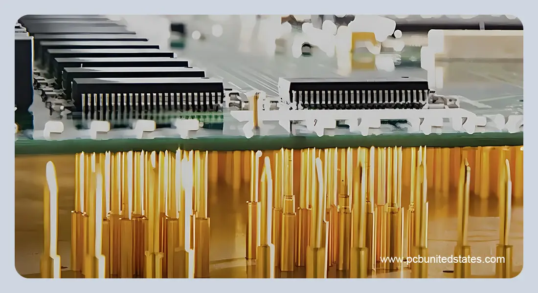
Bed-of-Nails: It consists of some spring-loaded contact pins (pogo pins) that contact specific test pads or vias on the PCB. These are temporary connections which enable the tester to send electrical signals and measure parameters of resistance, capacitance and continuity to detect short, open or wrong components.
Tester: A tester is the main component of ICT system, the one that generates electrical stimulus, and records the electrical response of a circuit under test. It integrates devices of voltage and current sources, digital multimeters, switching matrices and data acquisition modules and offers the possibility to understand the electrical performance of the board in detailed manner.
Fixture: A fix is needed to hold the PCB in place when the testing is operating and to provide the consistent contact between the test points and the bed-of-nails pins. It has a repeatable interface to ensure the correct electrical connections and to minimize the errors caused by misalignment or bad contact.
Software: The entire testing is organized following the ICT software. It defines the sequences of the tests, measures equipment, gathers and analyses data. It also provides diagnostic reports and analytics, which allow engineers to be capable of locating faults in a brief period of time and make production more efficient.
How Does In-circuit Test Work?
The circuit testing of PCB usually involves the following basic steps:
1.Test Setup
The initial one is to set a special bed-of-nails of those PCBs, which require testing. It contains spring loaded pins that go into the test points of the board and which are in reality actually correspond to a particular component or electrical node.
2.Test Program Development
This is an individualized test program where arrangements of the order of testing, measurement parameters and expected outcomes are determined. This software is programmed in a special programming language that is compatible with ICT systems.
3.Test Execution
The system provides electrical stimuli to the PCB with the responses being measured, when the setup and the program are complete. These signals are matched and compared to the expected reference values.
4.Measurement and Data Analysis.
Significant electrical parameters, such as the resistance, capacitance, inductance, values of current and voltage, and others, are measured in the testing and analyzed to find the accuracy and consistency.
5.Fault Identification
The ICT system identifies the faulty, an aspect or a node of the circuit, in case of any discrepancies. The diagnostic data is then relayed to engineers or technicians to be done.
6.Result Reporting
This will be the final step that will evaluate the procedure of documenting and storing all tests results. The same problems can be detected and eliminated using such reports as a reference point of quality control and also to identify the same in the next production cycle.
Common Defects Detected by In-Circuit Testing
In-circuit testing (ICT) helps detect critical fault that might interfere with the functionality and durability of a printed circuit board. Some of the most prevalent issues that it can detect are below:
- Power and Signal Integrity Issues: ICT checks if signal timing, voltage levels and signal quality are in compliance with design requirements. It is able to identify problems like noise, crosstalk, voltage drops or signal integrity problems.
- Defective Components: Damaged or faulty components like incorrect pin formation, malfunctioning ICs or broken diodes can be easily detected during the PCB in circuit test.
- Soldering Problems: ICT can also defects PCB solder issues such as cold joints, solder bridges, too much or too little solder, and unwanted solder splashes.
- Improper Component Placement: ICT confirms that every component is placed and oriented in the right way depending on the design of the board.
- Incorrect Component Values: In-circuit test can check electrical values of resistors, capacitors and inductors against their desired specifications.
- Short Circuits: It is a test that identifies unwanted electrical connections between conductors which can happen because of solder bridges or overlapping component leads.
- Open Circuits: ICT identifies broken or incomplete electrical paths, which can result from damaged traces, poor solder joints, or missing components.
Advantages and Disadvantages of In-Circuit Testing
Advantages
- Early Defect Detection: The ICT detects defects earlier on the assembly and does not allow defective boards to proceed into the subsequent manufacturing processes. This early detection saves repair costs and reduce scrap rates.
- High Test Coverage: ICT can measure single components, connections, and circuit values with a great precision and achieve up to 98 percent fault coverage on a well-designed printing board.
- Quick testing throughput: ICT can quickly test even complex PCBs once programmed, meaning it is suited for high-volume production environments where time is of the essence.
Disadvantages
- High Start-up Cost : ICT systems have high start-up expenses in equipment and special test fittings. In the meantime, bed-of-nails fixtures are time-consuming hence may slow down the pace of production.
- Maintenance Requirements: Calibration and normal maintenance of test fixtures are needed for ICT system, since test accuracy may be influenced by pin wear and damages in the long run.
- Unsuitable for Low Volume: In the case of prototype or low-volume manufacturing, the cost of the fixtures can outweigh the benefits, and other types of testing would be more economical.
ICT vs. Other Testing Methods: A Comparison Table
| Feature | In-Circuit Testing (ICT) | Flying Probe Testing | Functional Testing |
|---|---|---|---|
| Test Method | Bed-of-nails fixture with multiple probes | Moving probes test individual points | Tests complete board operation |
| Setup Cost | High (custom fixtures required) | Low (no fixtures needed) | Medium to High |
| Test Speed | Very fast (seconds per board) | Slow (minutes per board) | Medium (varies by complexity) |
| Best For | High-volume production | Low to medium volume, prototypes | Final product verification |
| Fault Coverage | 85–98% of manufacturing defects | 70–85% of manufacturing defects | 100% functional verification |
| Flexibility | Low (fixture per board design) | High (programmable for any design) | Medium (requires test programs) |
| Component Testing | Individual component values | Individual component values | Component interaction only |
| Test Point Requirements | Requires dedicated test points | Minimal test points needed | Requires operational interfaces |
| Cost Per Test | Very low | Medium | Medium to High |
| Programming Time | Medium | Short | Long (complex test scenarios) |
Contact MOKOPCB for Reliable PCB Testing
In-circuit testing is a necessary PCB testing method that saves money and shortens the manufacturing timeline, as well as ensures quality. At MOKOPCB, our comprehensive ICT system is incorporated into our full PCB manufacturing and assembly services. We go beyond standard testing—we use advanced equipment and strict inspection protocols to make sure that all boards strictly meet exact specifications. Work with MOKOPCB to experience PCB manufacturing with the support of industry-leading testing capabilities. Get in touch with us to find out more!
Contact Us
Got any questions or inquiries? Fill out the form and we will get back to you soon