Layer Stackup
As the trend of electronic product development is towards miniaturizing, lightweight, and multi-purpose, the application of the multi-layer PCBs is getting increasingly popular. PCB layer stackup, as the fundamental structural foundation of multi-layers circuit board design, has direct impact to signal integrity, power integrity, and performance. Whether working on a 2-layer board on basic applications, or a multi-layer PCB on high-speed digital systems, layer stackup is a key technology to know to achieve the best performance, and to maintain reliable operation.
What Is Layer Stackup?
Layer stackup refers to the layout and order of copper layers and insulating dielectric layers in a printed circuit board (PCB). It specifies the structure of the PCB prior to the layout design work. The stackup contains all the information required for the production of the PCB, including how many signal and power layers there will be, how thick the core and the prepreg materials will be, and the thickness (weight) of the copper.
The common PCB stack up is constructed with two main insulating materials, namely prepreg and core:
Prepreg, short for pre-impregnated, is a resin-coated fiberglass material that bonds layers together when heat and pressure are applied during lamination.
The PCB core is made of one or more layers of prepreg that are laminated, pressed and thermally cured into a solid substrate with copper foil on both sides.
These sheets are stacked in specific sequences to form multilayer PCBs that support electrical, thermal, and mechanical demands.
Why Stack-up Is Necessary in Multilayer PCB Design?
A well-designed stack-up assists in controlling signal integrity by maintaining consistent impedance and minimizing crosstalk, which also ensures reliable power distribution, and electromagnetic interference (EMI) reduction. Additionally, a proper stack-up contributes to effective heat dissipation, prevents board warping, and allows for a cost-effective design that can be manufactured easily by arranging signal, power, and ground layers in a logical way.
In contrast, poor PCB layer stackup design and the wrong choice of suitable material may present significant electrical performance problems in signal transmission, increased radiation and crosstalk, which makes the product more prone to external noise interference. These issues may lead to timing failures and interference, and ultimately lead to operational problems that considerably affect the performance and long-term reliability.
Our Standard PCB Layer Stackup
MOKOPCB has the standardized capability to produce multilayered PCBs up to 18 layers, with board thickness ranging from 0.3mm to 5.0mm, copper thickness ranging from 0.5 to 5oz, and minimum layer spacing of 4mil. Below are examples of our commonly utilized stack-ups:
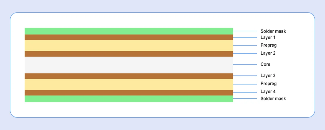
4-layer PCB stackup
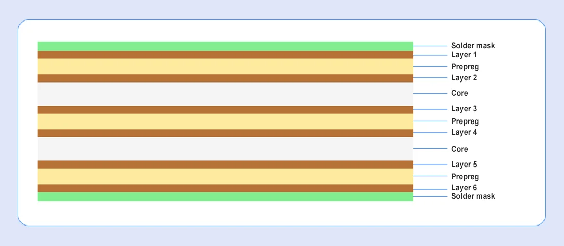
6-layer PCB stackup
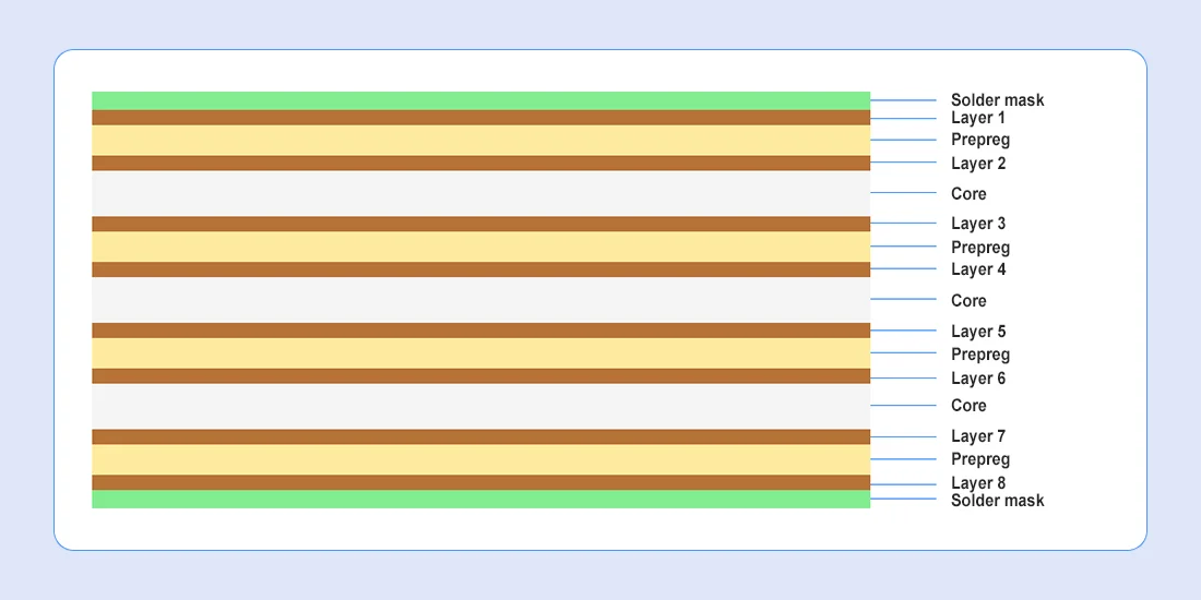
8-layer PCB stackup
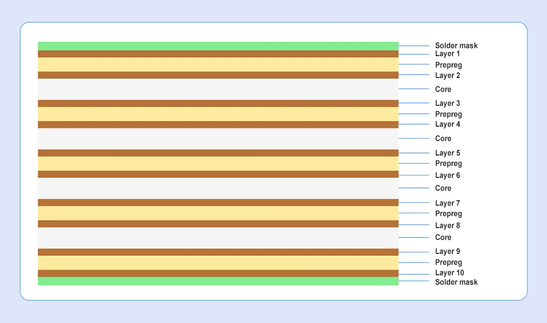
10-layer PCB stackup
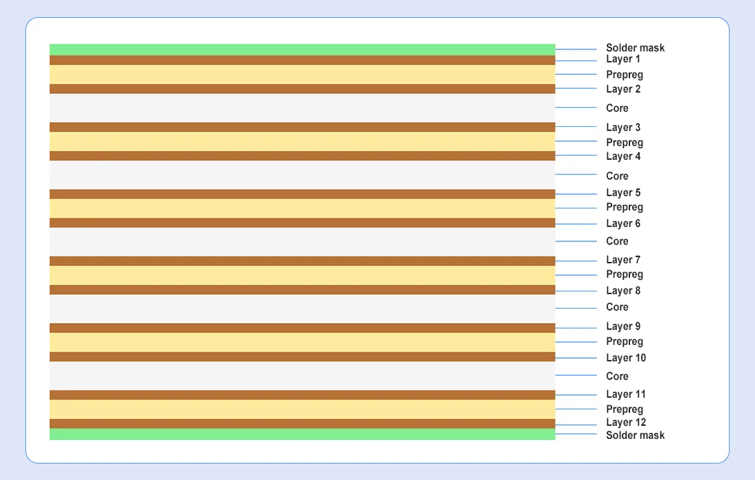
12-layer PCB stackup
The actual layer stack-up will depend on PCB material and numerous other factors. When you have special requirements for PCB layer stackup, just send us your circuit board thickness and the number of layers requirements. Our engineers will provide you with the corresponding stack-up.
5 Design Tips to Build an Efficient PCB Stack-up
- Select the Right Dielectric Material
The basis of PCB stack-ups design is material selection, which has a direct effect on the signal propagation as well as clock setting and heat management. When choosing dielectric materials, it’s critical to make sure they meet your electrical, mechanical, and thermal requirements. For example, if your circuit boards are used in high-frequency applications, then you should go for low dielectric constant materials that can minimize signal loss.
- Determine Optimal Signal Layer Count
The architecture of your PCB is largely determined by the number of signal layers and this directly influences the efficiency of routing. High-speed digital designs and power-intensive applications tend to have more layers than relatively simple circuitry. Some complex components like BGAs that have fine pitch and high pin counts would also require multiple signal layers for dense routing. Also, tight signal integrity requirements such as ultra low crosstalk targets may necessitate increasing the layer count to separate signals.
- Plan Ground and Power Plane Distribution
Signal layers are freed up by having dedicated ground and power planes, and DC resistance in power distribution networks is minimized, thus causing minimal voltage drop at component locations. Ground planes serve to provide necessary return paths for high-frequency signals, which reduces the electromagnetic interference and crosstalk considerably. Power planes enhance decoupling effectiveness by creating distributed capacitance across the board, improving the transient behavior and electromagnetic compatibility. To obtain optimal results, ground and power layers should be placed as close to each other as possible, so as to maximize distributed capacitance and ensure superior electromagnetic compatibility.
- Ensure Consistent Impedance Control
In high-speed designs, ensuring a consistent impedance is essential to ensuring signal integrity. To reach this, proper consideration of the trace parameters (width, spacing, and position in PCB stackup) is important. If a solid reference plane isn’t directly beneath a trace, nearby copper features may unintentionally serve as the return path, leading to signal distortion. To avoid this, it is critical to place a solid ground plane directly beneath impedance-controlled traces. Additionally, consider trapezoidal shape of etched traces when performing impedance calculations.
- Optimize Layer Sequencing to Reduce EMI
Strategic arrangement of the layers is critical in reducing the electromagnetic interference. Use alternating patterns of signal, ground and power planes to form effective shielding. Make sure that position signal layers very near to ground planes to achieve a tight electromagnetic coupling. There should be sufficient spacing between ground and power planes while avoiding adjacent signal layer placement. Maintain stackup symmetry to avoid warpage during the manufacturing process, and avoid segmented power planes that create noise coupling paths.
Choose MOKOPCB for Your PCB Layer Stack-Up Needs
MOKOPCB provides comprehensive PCB layer stack-up solutions and has expertise in design consultation, precise stack-up configuration, and material selection for multilayer PCBs. Our services begin with layer stack-up design, followed by prototyping and full-volume production. With nearly 20 years of manufacturing experience, we offer unparalleled speed, quality, and value in multilayer PCB manufacturing.
Ready to kick off your PCB project? Complete the form below to tell us your specific needs, and we’ll get back to you shortly.
Contact Us
Got any questions or inquiries? Fill out the form and we will get back to you soon