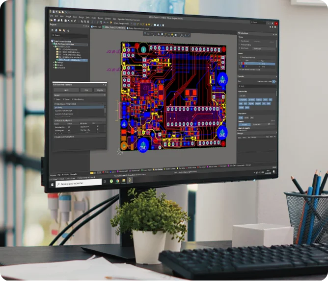
Requirements Analysis
Schematic Design
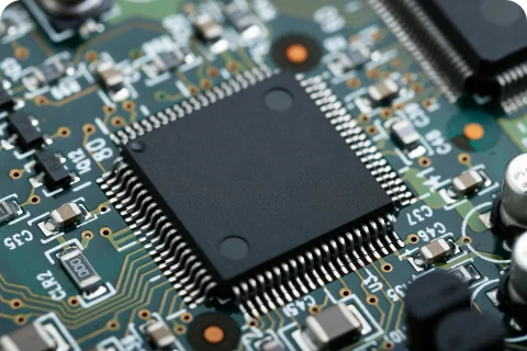
Component Selection
Layer Stack-up Design
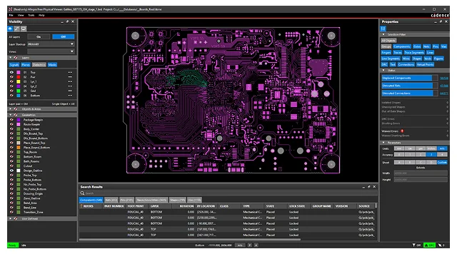
Design Verification
Signal Routing
Component Placement
Manufacturing File Generation


Expert Engineering Team
Experienced engineers
with diverse industry
backgrounds delivering
innovative solutions.
One-Stop PCB Solution
Seamless integration from design to manufacturing, assembly, and testing.
Fast Turnaround Time
Efficient processes and validated design modules for faster delivery.
Cost Optimization Expertise
Design optimization for cost-effective production without compromising quality.
High-Performance Computing Board
24-layer server mainboard with DDR4 and PCIe 4.0 interfaces, designed for enterprise data centers requiring maximum processing power and reliability.
Medical Monitoring Device
8-layer mixed-signal PCB for patient vital monitoring system with strict requirements for electrical isolation, EMI immunity, and medical certification standards.
Industrial IoT Control System
6-layer control board designed for harsh industrial environments with requirements for -40°C to +85°C temperature range, vibration resistance, and 10+ year operational lifespan.