PCB Solder Mask
PCB solder mask is the colored coating you can see on most printed circuit boards, usually green but also available in blue, black and other colors. Not only a cosmetic feature, this barrier layer is critical to the functionality, reliability and manufacturability of PCBs.
What Is PCB Solder Mask and Why Is It Critical?
Solder mask, solder resist, or solder stop mask is a thin film deposited on the top and bottom of a PCB. Although it gives PCBs a specific color, its primary role is much more than that: it protects copper traces against environmental threats and controls the soldering process.
The major advantages it offers are:
- It shields copper traces against moisture, chemicals, and electrolytes, which may cause oxidation and decrease conductivity.
- It safeguards the board against physical damage such as scratches that could cause accidental shorts.
- The solder flow is controlled in the assembly process so that solder is only applied to designated pads to avoid bridging between components.
- It makes PCBs more aesthetic, allowing them to be produced in various colors for identification or branding purposes.
Four Main PCB Solder Mask Types
The selection of the solder mask type should only be based on the application requirements, cost, and precision requirement. This is what you should know about each of the options:
1. Top and bottom masks
These masks identify openings made in the solder resist layer already applied to the PCB. Applied using epoxy or film methods, they produce registered openings in which component pins will be soldered. Top-side masks are used to cover the component side of the board, while bottom masks are used to protect the solder side.
2. Epoxy liquid solder masks
Epoxy masks are the most economical option, using a polymer that is silkscreened directly onto the PCB. A woven mesh is used in this printing process to support ink-blocking patterns, allowing ink to be accurately transferred to open areas.
3. Liquid Photoimageable Solder Mask (LPSM)
LPSM is a type of solder mask that is precisely applied using a photolithography process. It can be screen-printed or sprayed onto the board, and then exposed to ultraviolet (UV) light through a photomask created from Gerber files. UV exposure causes the mask to harden in desired areas while unexposed sections wash away, leaving openings for pads, vias, and holes. This technique ensures proper alignment and clean definition, making it the ideal choice for high-density and fine-pitch PCBs.
4. Dry film photoimageable solder resists
In this type of circuit board solder mask, a dry film layer is applied using vacuum lamination, followed by controlled exposure and developing procedures. Following development, openings are identified to create accurate soldering patterns for components. Dry film solder mask is especially common in high-density PCBs, as they prevent solder resist from entering through-holes, thus preserving good signal integrity.
Common Solder Mask Colors in PCB
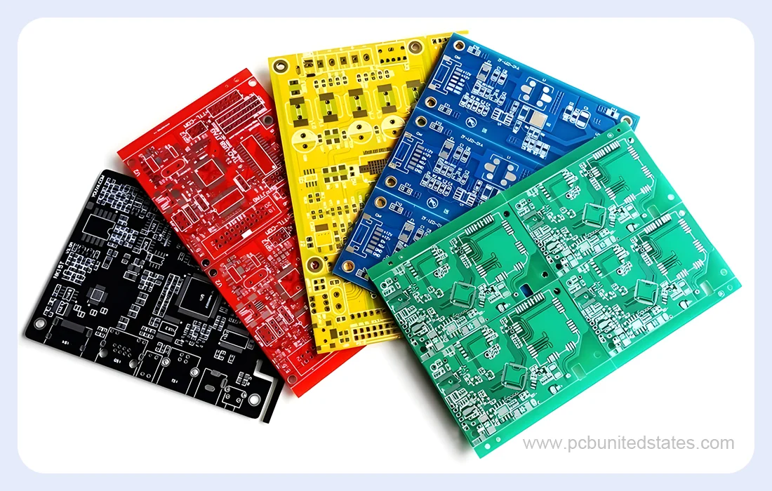
Although the industry standard is green, the modern PCB manufacturing process provides an array of color choices to satisfy multi-purpose and aesthetic needs. MOKOPCB offers seven colors:
Green: Standard industry selection that provides superior contrast for inspection, and has superior thermal/chemical resistance.
Blue:Good contrast against white silkscreen, popular in high-end consumer electronics.
Black: Provides sleek, professional appearance but may complicate inspection and absorb more heat.
Red: Chosen for aesthetic appeal or product differentiation with good visibility.
Yellow: Great brightness and thus easily identifiable, suitable to prototype or special uses.
White: Reflects light well, commonly used in LED lighting products.
Purple: Often selected for branding or specialty projects.
Standard Thickness of a Solder Mask Layer
The thickness of the solder mask layer is mostly decided by the thickness of the copper traces on the PCB. LPSM and DPSM solder mask thicknesses in areas without components vary at different locations. The normal solder resist thickness is greater than or equal to 0.8 mils. Solder mask may be as thin as 0.3 mils or less near the edges of traces. Generally, you will have approximately 0.5 mils of solder mask coverage over your traces. Epoxy solder mask can be sprayed to achieve a more consistent thickness all over your PCB.
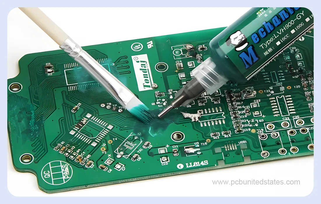
How Is Solder Mask Applied in PCB Manufacturing?
Step 1: Board Preparation
Thorough cleaning removes dirt and contaminants, followed by complete surface drying to ensure proper adhesion.
Step 2: Solder mask ink coating
The PCB is placed in a vertical coating machine where solder mask ink is applied. The coating thickness depends on various factors such as reliability requirements, and operating environment. The thickness may also differ across board sections—such as over traces, planes, or the substrate—and varies according to the manufacturing capabilities of the contract manufacturer.
Step 3: Pre-hardening
At this stage, the coated solder mask is partially cured to give it some rigidity. This pre-hardening makes it easier to remove the excess solder mask material in the next step.
Step 4: Imaging and UV Exposure
The solder mask pattern in the conventional imaging process is lasered-plotted on a photo film. It is a film that is well aligned to coated PCB panel which already has solder mask ink coated and is dried. After getting it aligned, the panel is exposed to ultraviolet (UV) light. The UV light transmits through the transparent parts of the film and cures the underlying ink so that it solidifies. On the contrary, the Laser Direct Imaging (LDI) technique does not require using photo films. Instead, the mask ink is cured on its intended position by a UV laser, thus simplifying the process and improving accuracy.
Step 5: Developing
The PCB is immersed in a developer solution that removes the excess solder resist, revealing only the intended copper areas for further processing.
Step 6: Final Curing and Cleaning
A final curing process fully hardens the remaining solder mask to ensure long-term durability. Afterward, the board is cleaned to prepare it for the next steps, such as applying the surface finish.
Solder Paste vs Solder Mask Layers: What’s the difference?
Solder Paste Layer: Solder paste layer is design file only utilized by stencil manufactures to make SMT stencils. This layer specifies the placement of solder paste on component pads when doing surface mount assembly of components. It does not participate in any real PCB manufacturing and it is not processed by PCB makers.
Solder Mask Layer: Solder mask layer is a parameter that will determine which sections of your PCB will be left as exposed copper and which areas will be covered by the solder resist.
Substantial Difference: The solder paste layer is only applied at the assembly stage; it is used as a stencil making guide that helps in applying the solder paste to the pads of the components during the SMT stage. By contrast, the solder mask layer is physically part of the PCB itself- it is applied directly to the board during PCB fabrication.
Partner with MOKOPCB for Consistent Solder Mask Performance
Professional solder mask application can be the key to the long-term reliability of your PCB. We deliver reliable PCB solder mask results throughout your entire production run by using controlled environments, precise UV exposure systems, and rigorous testing processes. Want to experience the difference that professional PCB solder mask manufacturing can make? Talk to our technical experts at MOKOPCB today.
Contact Us
Got any questions or inquiries? Fill out the form and we will get back to you soon