PCBA Process
PCB Assembly Capabilities
The PCBA process will make or break your electronic product during manufacturing. Although design faults can be addressed, assembly defects identified late in the run are 10 times more expensive to fix and can render an entire product launch a failure. Knowing every critical stage helps avoid expensive rework and achieve first-pass production. This guide explains the necessary steps involved in converting bare PCBs into functional electronic devices.
What Is PCBA?
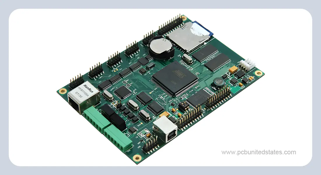
Printed Circuit Board Assembly is abbreviated as PCBA. The term refers to the manufacturing process whereby electronic components are soldered to a printed circuit board in order to make a complete and working circuit. The PCB provides mechanical support to the electronic product, a rigid platform on which the components are mounted, and provides electrical connections within the product. After the parts are successfully soldered to the board through the PCB assembly process, the final product is what we call a PCBA.
Preparation before PCB Assembly
There are some essential preparations prior to the actual assembly to ensure a smooth and error-free production process:
DFM Inspection
Prior to assembly, PCB design files undergo a Design for Manufacturability (DFM) review. This step assesses the functionality and manufacturability of the board and identifies design flaws at the early stages. By correcting errors and resolving issues in advance, manufacturers can avoid costly problems later and ensure a successful PCBA process.
Incoming Quality Control (IQC)
Once components arrive, they are carefully checked against the Bill of Materials (BOM) for accuracy in part number and quantity. Visual inspections are conducted to find defects like bent pins, oxidation, or deformities, which is especially important for ICs and other delicate or high-value components. In addition, tools like multimeters and test fixtures may be used for spot checks or full testing.
Equipment Setup and Programming
When the bare PCBs and all the required components arrive, engineers prepare them and program the machines used in the assembly. Automated placement machines like SMT placers and Automatic Optical Inspection machines have to be set up with precise configurations in order to work properly.
PCBA Process: 7 Key Steps Involved
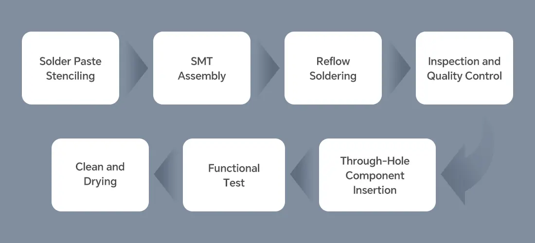
Printed Circuit Board Assembly is a meticulous process that converts a blank PCB into a fully-operational electronic component. The following are the seven major steps in the process:
Step 1: Solder Paste Stenciling
The PCBA process starts with solder paste stenciling. A thin stainless-steel stencil is placed over the PCB, and solder paste is applied only to pads where components will be mounted. This provides the correct positioning and good solder joints later in the process.
Step 2: SMT Assembly
The board then goes to the Surface Mount Technology (SMT) phase after the solder paste is applied. With automated machines, SMDs are placed directly on the pads that are covered with solder paste. Modern SMT lines can operate with high speed and accuracy, so as to reduce the errors that may arise when placing them manually. SMT assembly has become the standard for most electronic products because it enables miniaturization, higher component density, and faster production.
Step 3: Reflow Soldering
When SMDs are placed, the board is then reflow soldered. The PCB is placed on a conveyor and enters a reflow oven and is heated to around 250°C until the solder paste melts. When cooled in a controlled process, the solder solidifies and durable electrical and mechanical connections are formed. In the case of double-sided assemblies, this process is repeated for both sides.
Step 4: Inspection and Quality Control
Inspection is carried out after reflow to determine whether the components are soldered and placed appropriately. Common methods include:
Manual inspection: Visual inspection by trained technicians is still common for small batches or prototypes. Inspectors use tools such as magnifying glasses and microscopes to detect flaws like solder bridges, misaligned parts, and missing components.
Automated Optical Inspection (AOI): In case of high-volume production, the use of AOI machines is preferred. These machines operate the high-resolution cameras in order to take the images of the PCB at various angles. The images are analyzed through software and issues like inadequate solder, lifted pads, or displaced parts can be identified.
X-ray Inspection: X-ray inspection is used for boards with complicated parts such as BGAs ( Ball Grid Arrays ) or dense multilayer layouts where solder joints are hidden beneath the component. With this method, engineers can look through the board and check these hidden connections. This process makes sure that internal solder joints are of good quality without damaging parts.
Step 5: Through-Hole Component Insertion
Through-hole components are sometimes needed, such as connectors or large capacitors. These components incorporate plated through holes (PTHs) to make signal connections between layers. Solder paste is not suitable in this case and other soldering methods are used in the PCBA process:
Manual soldering: Manual soldering is performed by inserting each of the components into a specific hole and soldering it manually. This method is flexible, enabling the exact handling of components with irregular shapes or those that demand special orientation. Manual soldering is usually applied in low-volume manufacturing, prototyping, or complex assemblies.
Wave soldering: For higher-volume production, wave soldering automates the process. Boards with inserted through-hole components are passed over a wave of molten solder, which touches the underside of the board and solders all pins simultaneously. This process is effective and gives reliable uniform solder joints. However, it is usually suitable for single-sided or selectively populated double-sided printed boards since the components in the other side can be damaged by heat or the flow of solder.
Step 6: Functional Test
Next, functional testing is undertaken. In this test, the board is powered on in simulated working status. Electrical loads and signals are applied, and the engineers validate that the PCB functions as expected. This step is necessary as it confirms that all connections are accurate and the board is operational before it is delivered.
Step 7: Clean and Drying
Finally, any flux residue, solder paste, or dirt is removed. Boards are cleaned with deionized water or ultrasonic methods, then dried using compressed air. This final step of the PCB assembly process improves both appearance and long-term reliability, as contaminants can cause corrosion or electrical faults over time.
PCB Assembly Service at MOKOPCB
With years of industry experience and advanced facilities, MOKOPCB is able to provide reliable and precise PCB assembly services. Equipped with 5 SMT lines and 3 DIP lines, we have flexible manufacturing capabilities to handle both prototypes and mass production with fast turnaround.
Moreover, we carry out strict quality control processes, and are certified with ISO9001, ISO13485, UL, RoHS, etc. Whether it’s simple circuit boards or complex multilayer boards with fine-pitch components, we can meet the highest quality standards.
From design review to final functional testing, MOKOPCB provides one-stop PCB assembly solutions to help our clients bring their electronic products to market. Contact us now to discuss your PCB assembly project!
Contact Us
Got any questions or inquiries? Fill out the form and we will get back to you soon