Advanced HDI PCB Manufacturing Delivering Exceptional Density and Performance.
Partner with MOKOPCB for Advanced HDI PCB Solutions
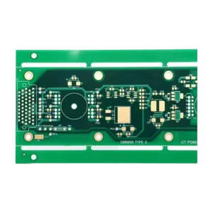
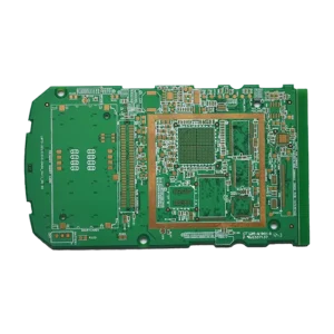
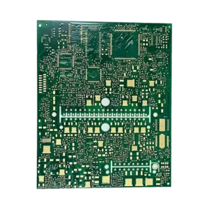
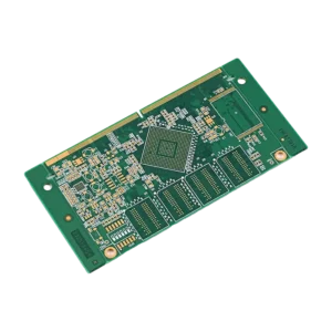
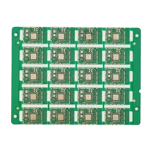
MOKOPCB produces high-performance HDI PCB solutions that specifically address the needs of modern compact electronic products requiring high speed operations. By integrating the sophisticated manufacturing techniques such as laser-drilled microvias, ultra-fine line/space, multi-layers constructions, we offer HDI PCBs that have quality signal integrity, low EMI, and high reliability. MOKO is your go-to HDI PCB manufacturer with experienced engineering team, strict quality assurance and fast delivery time.
We provide a full range of PCB solutions which includes design services alongside fabrication and sourcing and delivery to save your time and expenses.
Strict Quality Control
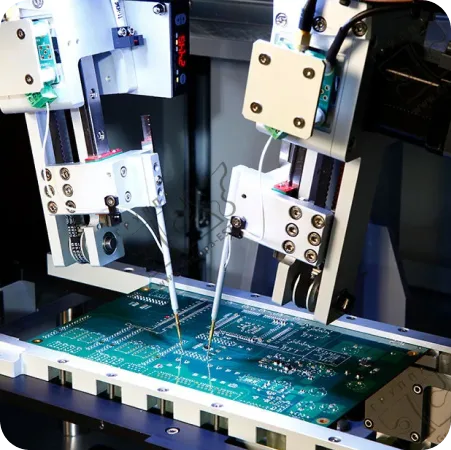
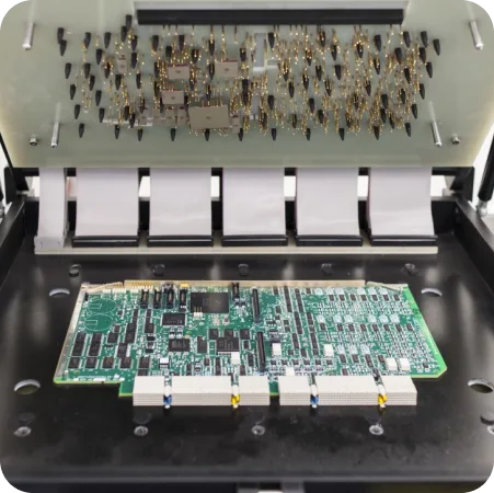
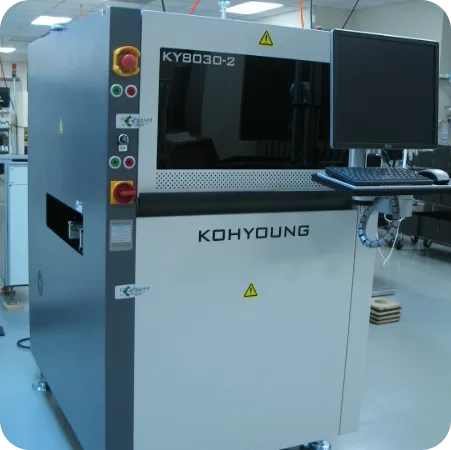
MOKOPCB implements advanced PCB inspection techniques and follows the ISO standards to make sure that all boards fulfill strict reliability and quality requirements.
Manufacturing Expertise
MOKOPCB’s seasoned engineers and advanced facilities ensure reliable production of high-quality PCBs across diverse materials, layers, and complexities.
Production Flexibility
Our company accepts urgent orders together with customized specifications and fluctuating order quantities while maintaining quality standards and delivery timeliness.
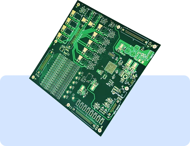
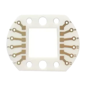
HDI PCB, with the full name of High-Density Interconnect PCB, is a type of circuit board that has higher wiring density per unit area than normal PCBs. Additionally, it is featured with small vias, finer lines and spaces.
What are the advantages of HDI printed circuit boards?
HDI printed circuit boards has many advantages such as compact size, fast signal transmission speed and better thermal management.
What industries benefit most from HDI PCB boards?
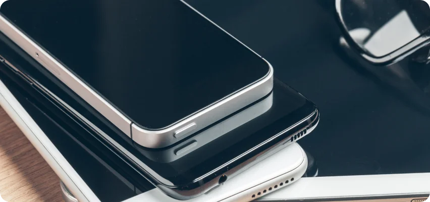
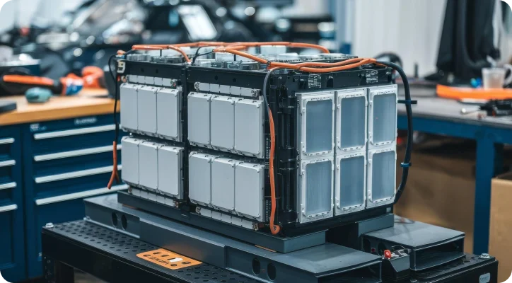
HDI features high miniaturization and reliable performance, making it very beneficial to industries like telecommunications, consumer electronics, automotive and medical devices.
What HDI design capabilities does MOKOPCB offer?
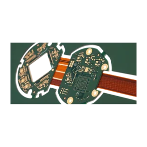
MOKOPCB provides professional HDI PCB design that encompass stacked microvias along with buried vias and blind vias and advanced layer counts and support for fine pitch components.
What types of HDI printed circuit boards do you manufacture?
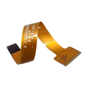
At MOKOPCB, we have the ability to manufacture HDI printed circuit boards from single layer to 10+ layers with various microvia structures (stacked, staggered, and buried), and advanced material compositions for high frequency applications.
How does MOKOPCB ensure the quality of PCBs?
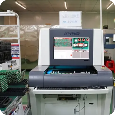
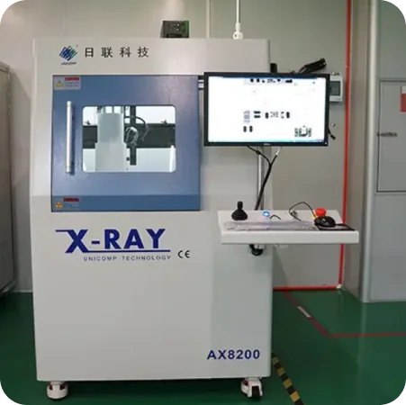
MOKOPCB uses advanced quality control systems and a series of testing methods such as Automated Optical Inspection (AOI) and X-ray inspection alongside electrical testing for achieving the highest quality.
Contact Us
Got any questions or inquiries? Fill out the form and we will get back to you soon