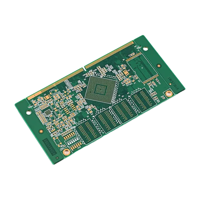
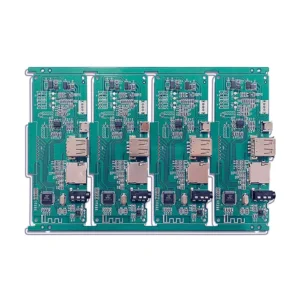
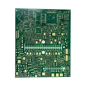
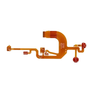
6 layer HDI PCB with microvia technology
$36.50
6 layer HDI PCB is a type of multilayer circuit board with six conductive layers, which adopts high density interconnect technology to increase the routing density per unit area. This technology enables circuit boards to integrate more components and support complex tracing routing by using microvias, blind/buried vias, and finer trace widths and spacing. Compared with four layer HDI PCBs, 6-layer HDI PCBs have extra layers to increase routing flexibility, reduce via usage, and save space.
Shipping fee and delivery date to be negotiated. Send inquiry for more details.
Your payment information is processed securely. We do not store credit card details nor have access to your credit card information.
Claim a refund if your order is missing or arrives with product issues, our support team would deal with your refund within 24 hours.
| Layer Counts | 6L |
| Base Material | FR4 |
| Board Thickness(mm) | 1.0 |
| Max board size(mm) | 570*670 |
| PCB size tolerance | ±0.3mm |
| Min. Hole Size | 0.15mm |
| Min. Line Width | 4mil |
| Copper Weight | 2oz |
| Surface Finish | ENIG |
| Certificate | UL, RoHS, ISO, and REACH |
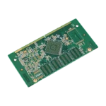 6 layer HDI PCB with microvia technology
| 5 star | 0% | |
| 4 star | 0% | |
| 3 star | 0% | |
| 2 star | 0% | |
| 1 star | 0% |
Sorry, no reviews match your current selections
Questions & Answers
1.What delivery options are available?
We provide multiple shipping solutions such as express delivery, air freight, and sea freight, depending on your timeline and specific needs.
2.Do you support different surface finishes?
Yes, we provide several surface finish options including HASL, ENIG, ENEPIG, OSP, immersion silver, and immersion tin.
3.What is the typical stack-up of 6 layer HDI circuit board?
A typical 6-layer HDI PCB stack-up usually consists of two outer signal layers, two inner signal layers, and two power or ground layers in the middle.
4.How to effectively manage heat dissipation in a 6 layer HDI PCB?
There are many ways to effectively manage the heat dissipation of 6-layer HDI circuit boards, such as selecting high thermal conductivity materials, optimizing the layer stack-up design, and using heat sinks or thermal vias.
5.Can a 6-layer HDI PCB board support rigid-flex designs?
Of course! 6-layer HDI PCB can support rigid-flex designs, providing flexibility while maintaining high density interconnect capabilities.

