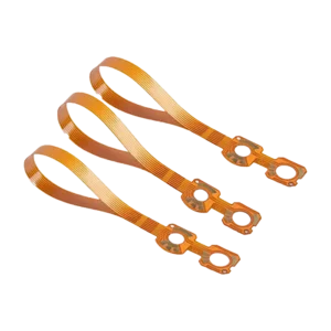
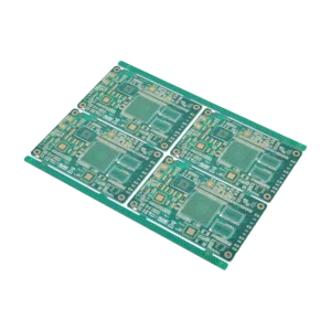
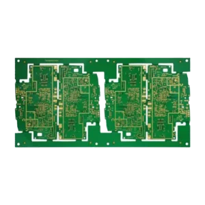
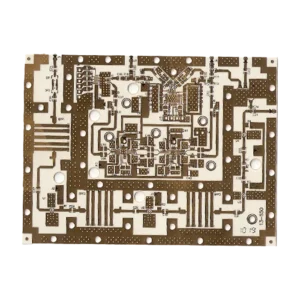
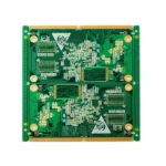
8-layer Customized High Frequency PCB
$129.90
High frequency PCB or HF PCB is specially designed for high-frequency signals operating usually at frequencies from 500MHz to high 100GHz and processes electrical signals with minimal loss and interference. They are widely used in modern industries, such as radar systems, satellite communications, 5G networks, and more. The production of HF PCB necessitates the use of specialized materials and processes, which makes it more expensive than standard PCB. MOKOPCB supports customized high-frequency PCB with high quality and a reasonable price.
Shipping fee and delivery date to be negotiated. Send inquiry for more details.
Your payment information is processed securely. We do not store credit card details nor have access to your credit card information.
Claim a refund if your order is missing or arrives with product issues, our support team would deal with your refund within 24 hours.
| Layer Counts | 8L |
| Base Material | Rogers |
| Board Thickness(mm) | 2.0mm |
| Max board size(mm) | 570*670mm |
| PCB size tolerance | ±0.2mm |
| Min. Hole Size | 0.15mm |
| Min. Line Width | 4mil |
| Copper Weight | 1oz |
| Surface Finish | ENIG |
| Certificate | UL, RoHS, ISO, ISO9001, ISO13485, IPC610, and REACH |
 8-layer Customized High Frequency PCB
| 5 star | 0% | |
| 4 star | 0% | |
| 3 star | 0% | |
| 2 star | 0% | |
| 1 star | 0% |
Sorry, no reviews match your current selections
Questions & Answers
1. What is the maximum board size for an 8-layer PCB?
The maximum board size is 570*670mm for 8-layer PCBs.
2. What is your lead time?
1-2 days. We have our own warehouse and stock in large quantities.
3. What are your payment terms?
T/T, Paypal, Western union, L/C, ESROW.
4. How does the temperature impact high frequency PCB performance?
When temperature increases, Dk and Df of the PCB material will vary to change signal transmission speed and cause signal loss. Thermal expansion mismatches between the dielectric substrate and traces may cause mechanical stress, leading to potential delamination.
5. What are the properties of high-frequency PCB?
High frequency PCB is characterized by low dielectric constant(Dk) and Low dissipation factor (Df), which reduces signal loss and maintains signal integrity. It also possesses stable thermal management to withstand operating heat and controlled impedance to decrease skin effect losses.
6. What are the challenges in fabricating multi-layer high-frequency PCBs?
Multi-layer HF PCB like this 8-layer HF PCB needs precise alignment, accurate drilling and planting, controlled impedance, and specialized materials selection.
7. What’s the guideline for designing a high-frequency PCB?
When designing a high frequency, our expert will help optimize your PCB layout to provide the best performance. Traces width for impedance control, trace length and direction for signal transmission, proper ground plane for anti-crosstalk, thermal management designs, and material selection, all these parameters should be considered carefully.
8. What signals does the high-frequency circuit deal with?
High-frequency circuits handle RF and microwave signals, high-speed digital signals, and wireless communication signals.
9. What applications are the high-frequency PCBs used in?
High frequency PCBs are widely utilized in those applications: cellular networks, communications systems, radar systems, automotives, medical devices, scientific tools, industries, consumer electronics, and transportation.


