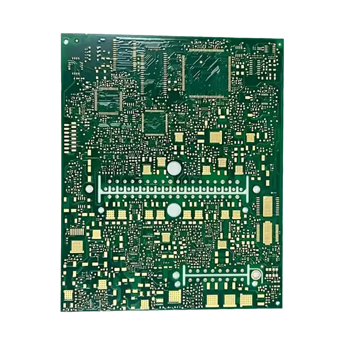
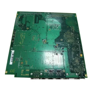
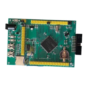
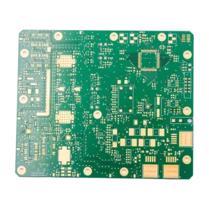
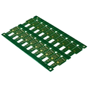
Low-cost 8 layer HDI PCB prototype for miniaturized design
$42.80
MOKOPCB is a China PCB prototype & PCB manufacturer that provides one-stop PCB and PCBA services, including providing 8 layer HDI PCB prototype services. You can get a high-quality 8 layer HDI PCB prototype at a low cost for testing and evaluating PCB design. This can ensure all potential problems are discovered and resolved prior to production.
Shipping fee and delivery date to be negotiated. Send inquiry for more details.
Your payment information is processed securely. We do not store credit card details nor have access to your credit card information.
Claim a refund if your order is missing or arrives with product issues, our support team would deal with your refund within 24 hours.
| Layer Counts | 8L |
| Base Material | FR4 |
| Board Thickness(mm) | 1.2 |
| Max board size(mm) | 570*670 |
| PCB size tolerance | ±0.3mm |
| Min. Hole Size | 0.15mm |
| Min. Line Width | 4mil |
| Copper Weight | 2oz |
| Surface Finish | ENIG |
| Certificate | UL, RoHS, ISO, and REACH |
 Low-cost 8 layer HDI PCB prototype for miniaturized design
| 5 star | 0% | |
| 4 star | 0% | |
| 3 star | 0% | |
| 2 star | 0% | |
| 1 star | 0% |
Sorry, no reviews match your current selections
Questions & Answers
1.What quality standards do you follow?
MOKOPCB follows strict quality standards like IPC-A-600 for PCB production and IPC-A-610 for assembly quality assurance.
2.What kinds of inspections are carried out on PCBs?
We perform various inspections such as AOI, x-ray, in-circuit testing, functional testing, and flying probe testing to ensure product quality.
3.What is the maximum PCB size you can support?
We support the following maximum PCB sizes: 570×1200 mm for double-sided boards, 570×850 mm for four-layer boards, and 570×670 mm for six-layer and above boards.
4.What are the common challenges in manufacturing 8 layer HDI PCB prototype?
Manufacturing an 8 layer HDI PCB prototype presents challenges related to accurate microvias drilling, layer-to-layer alignment, and uniform lamination quality.

