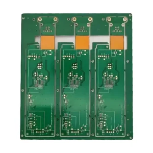
China Multilayer PCB
$59.90
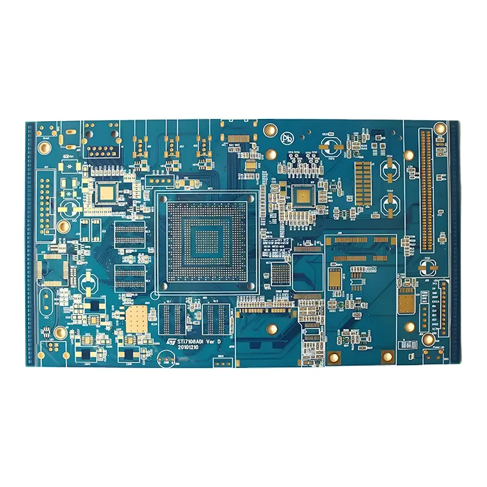
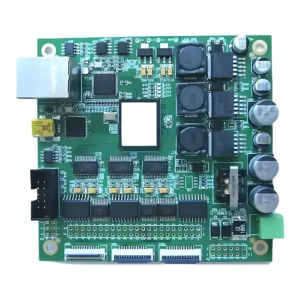
China Multilayer PCB manufacturers like MOKO provide high quality and cost-effectiveness. Multilayer PCB, typically 4 to 50+, has complex circuit designs with higher component density, offering better signal integrity and improved power distribution.
Shipping fee and delivery date to be negotiated. Send inquiry for more details.
Your payment information is processed securely. We do not store credit card details nor have access to your credit card information.
Claim a refund if your order is missing or arrives with product issues, our support team would deal with your refund within 24 hours.
| Layer Counts | 8L |
| Base Material | FR4 |
| Board Thickness(mm) | 2.0mm |
| Max board size(mm) | 570*670mm |
| PCB size tolerance | ±0.2mm |
| Min. Hole Size | 0.15mm |
| Min. Line Width | 4mil |
| Copper Weight | 2oz |
| Surface Finish | ENIG |
| Certificate | UL, RoHS, ISO, ISO9001, ISO13485, IPC610, and REACH |
 China Multilayer PCB
| 5 star | 0% | |
| 4 star | 0% | |
| 3 star | 0% | |
| 2 star | 0% | |
| 1 star | 0% |
Sorry, no reviews match your current selections
Questions & Answers
1. What is your lead time?
1-2 days. We have our own warehouse and stock in large quantities.
2. Why does the trace width vary in multiple PCBs?
Trace widths vary based on various factors, such as current flow, signal integrity, EMI, and thermal control. Wider trace width is designed to handle high current, and a thick trace width can be used for signal routing or high-density design. Our designers will adjust trace widths based on your specific requirements to achieve the best performance.
3. What tests are mandatory for 8-layer PCBs?
The mandatory tests generally include electrical tests for verifying circuit continuity, like flying probe or bed-of-nails testing; impedance testing for signal integrity; thermal stress test for assessing PCB’s durability under high temperature; and microsection analysis for checking internal layer alignment. Other tests include automated Optical Inspection (AOI), HALT (Highly Accelera Life Testing), ionic contamination checks, and more.
4. FR4 or Rogers, which one should I choose?
Choose FR4 if the budget is limited or it is used for normal purpose PCBs with moderate electrical performance. Rogers is pricer, but it is crucial for high-frequency RF/microwave applications as it has a low dielectric loss and stable Dk, such as radars, intercommunication systems, 5G, and more. However.
5. Why should I choose multilayer PCBs over single- or double-sided boards?
With more complex routing and internal power and ground planes, multilayer PCBs reduce noise and improve thermal management. They also save space and weight with higher circuit density, better signal integrity, and reduced EMI, making it ideal for cimpact and high-performance devices like medical equipment, aerospace, and consumer electronic devices. Those properties are not satisfied in single- or double-sided boards.
6. How does layer stacking affect signal integrity?
Layer stacking directly influences the signal integrity as it impacts impedance control, crosstalk, and power distribution. If the stackup is not well designed, it may cause impedance mismatching, increase crosstalk, and lead to interrupted return paths for high-speed signals.
7. How do you ensure reliable layer alignment in multilayer PCBs?
Reliable layer alignment in multilayer PCB is fundamental for proper via connections and impedance consistency. Fiducial marks and optical alignment systems ensure accurate registration before laminimation, and the controlled temperature and pressure preclude shifting during bonding. Post-production testing and inspection are also necessary, such as X-ray drilling and automated optical inspection.
8. What’s the difference between a core and prepreg in multilayer PCBs?
Core is rigid and pre-cured laminates that deliver structural support and fix dielectric thicknesses. Prepregs are semi-cured sheets of fiberglass and resin. Prepreg bonds cores together during lamination and fills gaps under heat and pressure. Cores maintain mechanical stability, and prepregs are flexible to stack layers and adjust thickness. Both are essential for a reliable multilayer board.
9. What’s the smallest through-hole you can drill?
The smallest through-hole size that MOKOPCB can drill is 0.15mm at the limit. We also support standard 0.3mm to 2.5mm holes according to specific needs.

