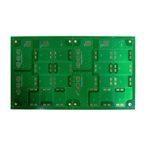
Custom Multilayer RF and Microwave PCB
$78.90
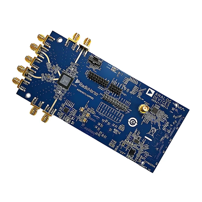
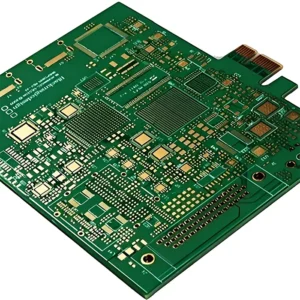
Multilayer RF and microwave PCB is complex with multiple layers of conductive material separated by dielectric substrates. MOKOPCB supports customizing Multilayer RF and microwave PCBs with superior signal integrity, exceptional thermal management, and optimal performance in various RF and microwave industries.
Shipping fee and delivery date to be negotiated. Send inquiry for more details.
Your payment information is processed securely. We do not store credit card details nor have access to your credit card information.
Claim a refund if your order is missing or arrives with product issues, our support team would deal with your refund within 24 hours.
| Layer Counts | 8L |
| Base Material | Rogers |
| Board Thickness(mm) | 2.0mm |
| Max board size(mm) | 570*670mm |
| PCB size tolerance | ±0.2mm |
| Min. Hole Size | 0.15mm |
| Min. Line Width | 4mil |
| Copper Weight | 3oz |
| Surface Finish | ENIG |
| Certificate | UL, IPC-6012, RoHS, ISO 9001, ISO14001 |
 Custom Multilayer RF and Microwave PCB
| 5 star | 0% | |
| 4 star | 0% | |
| 3 star | 0% | |
| 2 star | 0% | |
| 1 star | 0% |
Sorry, no reviews match your current selections
Questions & Answers
1. What is your lead time?
1-2 days. We have our own warehouse and stock in large quantities.
2. What is the maximum layer count MOKOPCB can produce?
We can produce up to 40-layer PCBs.
3. Where does MOKOPCB ship from and to?
We deliver our goods from our facilities in Shenzhen, China.
4. What’s the minimum copper thickness for vias in multilayer RF PCBs?
The minimum via thickness for buried and blind vias is on average 20um.
5. Can you mix RF and digital layers in an 8-layer PCB?
Yes. RF and digital layers can coexist in an 8-layer PCB but need careful stackup. RF signals should occupy dedicated layers with ground planes, and the digital signals can be routed in inner layers with proper shielding.
6. What solder mask options work best for multilayer RF PCBs?
The best solder masks for multilayer RF PCB we recommend are Tamura SF3055 and Taiyo PSR-4000. They are thin and halogen-free with a low-Dk to maintain signal integrity.
7. What’s the thinnest RF PCB you can manufacture?
We can manufacture 0.2 mm-thick RF PCB at the limit.
8. How many layers do you recommend for 40+ GHz radar PCBs?
For a 40+ GHz radar PCB, an 8-layer stackup is typically recommended. 8 layers can achieve great signal performance and reduce dispersion and manufacturing challenges.
9. How do you handle heat dissipation in multilayer high-power RF PCBs?
To better manage heat, we design the PCB with suitable materials(Rogers or metal core), use thicker copper for power traces, and drill thermal vias under hot components. In some special cases, we may use some advanced techniques like embedded heat sinks or metal-core boards to achieve reliability.

