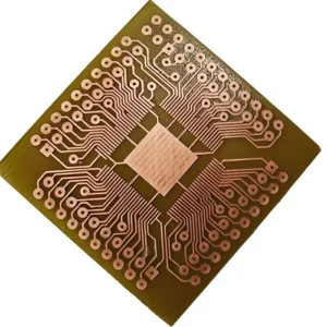
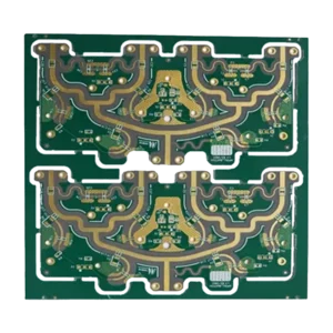
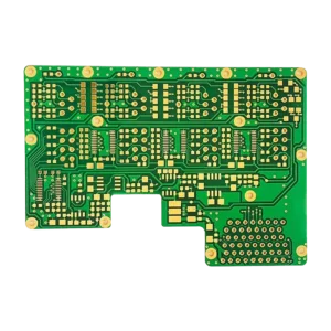
FR4 Multilayer PCB
$48.90
FR4 multilayer PCB provides optimized signal integrity, power distribution, and EMI shielding than single or double layer PCBs, making it feasible for reliable performance in electronics, including HDI, medical, aerospace, and high-speed digital circuits. MOKOPCB supports customizing various stackup PCBs up to 40 layers.
Shipping fee and delivery date to be negotiated. Send inquiry for more details.
Your payment information is processed securely. We do not store credit card details nor have access to your credit card information.
Claim a refund if your order is missing or arrives with product issues, our support team would deal with your refund within 24 hours.
| Layer Counts | 6L |
| Base Material | FR4 |
| Board Thickness(mm) | 1.0mm |
| Max board size(mm) | 570*670mm |
| PCB size tolerance | ±0.2mm |
| Min. Hole Size | 0.15mm |
| Min. Line Width | 4mil |
| Copper Weight | 1oz |
| Surface Finish | ENIG |
| Certificate | UL, RoHS, ISO, ISO9001, ISO13485, IPC610, and REACH |
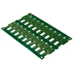 FR4 Multilayer PCB
| 5 star | 0% | |
| 4 star | 0% | |
| 3 star | 0% | |
| 2 star | 0% | |
| 1 star | 0% |
Sorry, no reviews match your current selections
Questions & Answers
1. What is your shipping port?
We ship the goods via the Port of Hong Kong or Shenzhen.
2. What are the power layer, signal layer, and ground plane in the PCB design?
The power and signal layer is both a specific layer within the PCB stackup. The power layers with copper planes transfer electrical power to various components on the PCB, like capacitors. Signal layers with copper traces are used to route electrical signals between components. Ground planes with complete copper planes provide return paths and reduce noise.
3. What factors determine the cost of a 6-layer FR4 PCB?
The cost of a 6-layer FR PCB varies with various factors, including board size, copper thickness, material, and surface finish. Raised fabrication costs include tight trace and spacing, precise vias, and impedance control. All in all, performance, tolerance, and protection efficiency determine the final cost.
4. What’s the ‘via in pad’ option for 6-layer PCBs?
Via-in-pad allows vias to be placed directly on the copper pads of surface mount components. This results in a more compact layout and improved routing efficiency, making it usually used in high-speed electronic devices to optimize signal integrity and reduce signal distortion.
5. What’s the thickness of a 6-layer FR4 PCB?
The thickness of a 6-layer FR4 PCB ranges from 0.8mm to 3.0mm, and the standard thickness is 1.6mm.
6. What’s the typical 6-layer FR4 PCB stackup?
The typical stackup is Signal/ Ground plane/ Signal or Power/ Signal/ Ground plane/ Signal.
7. Why is FR4 the most common PCB material?
FR4 is a flame-retardant epoxy-glass laminate. Its low cost, balanced electrical properties, and sound mechanical strength make it widely used in various PCBs for different applications.
8. Why does FR4 absorb moisture, and how does it impact manufacturing?
FR4 absorbs moisture because its hygroscopic epoxy resin and glass fiber weave can trap water. Moisture absorption may cause cracking during high-temperature soldering and degrade electrical performance. Workers need to prebake PCBs for 2-4 hours before assembly to evaporate absorbed moisture and store them in vacuum-sealed bags to avoid moisture.
9. What causes delamination in FR4 multilayer PCBs?
Delamination in FR4 multilayer PCBs may be caused by thermal stress, moisture absorption, poor laminations, or CTE mismatches.


