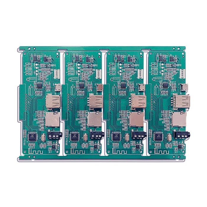
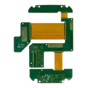
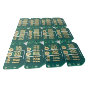
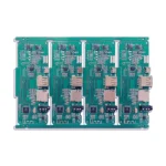
High frequency PCB 6 layer
$105.00
6-layer high-frequency PCB operates at high frequencies like RF, mmWave, and high-speed digital, maintaining signal quality and minimizing losses. 6-layer HF PCB offers greater signal integrity, enhanced EMI shielding, and power delivery. Such a 6-layer HF PCB is feasible for mmWave, 5G, high-speed digital, aerospace, and radar.
Shipping fee and delivery date to be negotiated. Send inquiry for more details.
Your payment information is processed securely. We do not store credit card details nor have access to your credit card information.
Claim a refund if your order is missing or arrives with product issues, our support team would deal with your refund within 24 hours.
| Layer Counts | 6L |
| Base Material | Rogers |
| Board Thickness(mm) | 1.6mm |
| Max board size(mm) | 570*670mm |
| PCB size tolerance | ±0.2mm |
| Min. Hole Size | 0.15mm |
| Min. Line Width | 4mil |
| Copper Weight | 1oz |
| Surface Finish | ENIG |
| Certificate | UL, RoHS, ISO, ISO9001, ISO13485, IPC610, and REACH |
 High frequency PCB 6 layer
| 5 star | 0% | |
| 4 star | 0% | |
| 3 star | 0% | |
| 2 star | 0% | |
| 1 star | 0% |
Sorry, no reviews match your current selections
Questions & Answers
1. What solder mask color do you provide?
We provide Green, Red, Yellow, Blue, White, Black, and Purple.
2. How does 6-layer high-frequency PCB mitigate EMI?
6-layer stackup makes use of solid ground planes to shield RF signals and reduce radiation. The stackup designs include dedicated signals, ground planes, and power planes to control impedance and minimize crosstalk.
3. Why is the 6-layer HF PCB the ideal choice for RF?
6-layer HF PCB provides specific ground planes between signal layers, reducing the influence of crosstalk and EMI and ensuring stable impedance control. Other layers also support dense RF wiring, shielding, and distribution, which is super important for GHz frequency circuits like radar.
4. How does 6-layer HF PCB thermal management work?
Copper planes can transfer heat away, and the thermal vias under heat-generating components also act as heat spreaders, transferring heat to the inner ground and power planes. Strategic component placement and thermally conductive Rogers can also manage heat.
5. How does moisture affect the HF PCB performance?
PTEE material of HF PCB can absorb moisture, increasing dielectric constant(Dk) and loss tangent, and degrading signal integrity. Hydrophobic coatings like Rogers or protective coatings can solve it. MOKOPCB primarily uses Rogers to avoid moisture influence.
6. Can you mix blind and buried vias with through-hole vias in a 6-layer stack-up?
Yes, we are capable of mixing them in a 6-layer HF PCB, but it needs careful design for best performance and cost. When designing vias, it is better to use blind and buried vias for RF signals and use through-hole vias for non-critical paths. Avoid unnecessary via layers in case of increased complexity and cost.

