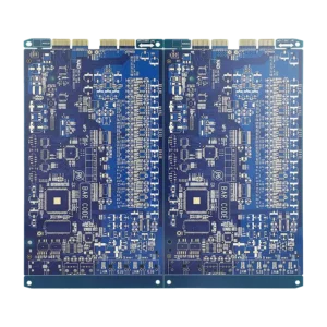
Wireless Charger PCBA
$40.90
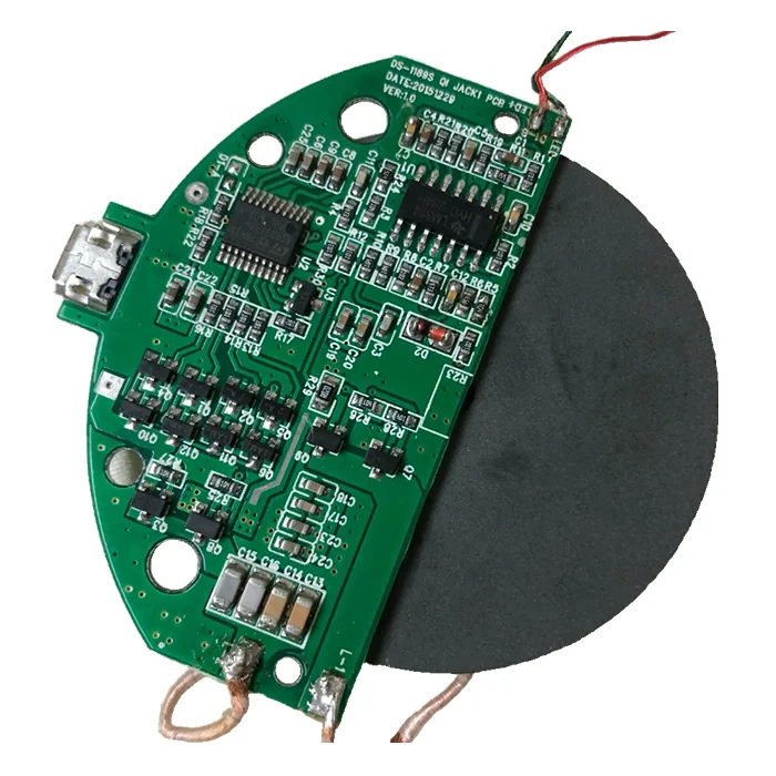
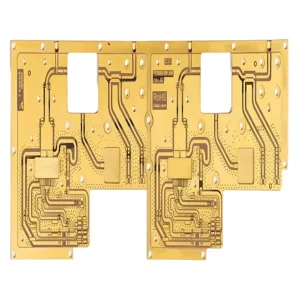
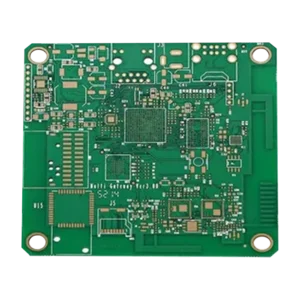
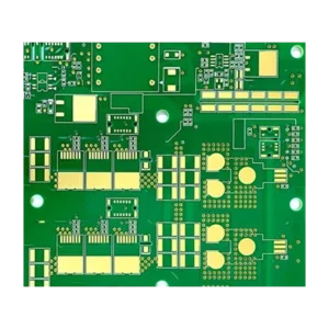
Wireless charger PCBA is the core electronic component inside a wireless charging device used for wireless power transfer. Reliable PCB design ensure high-efficient power transfer, minimal heat generation, and stable operation, ensuring safe charging without the need for physical connectors.
Shipping fee and delivery date to be negotiated. Send inquiry for more details.
Your payment information is processed securely. We do not store credit card details nor have access to your credit card information.
Claim a refund if your order is missing or arrives with product issues, our support team would deal with your refund within 24 hours.
| Layer Counts | 6L |
| Base Material | FR4 |
| Board Thickness(mm) | 1.6mm |
| Max board size(mm) | 570*850mm |
| PCB size tolerance | ±0.2mm |
| Min. Hole Size | 0.15mm |
| Min. Line Width | 4mil |
| Copper Weight | 2oz |
| Surface Finish | ENIG |
| Certificate | UL, RoHS, ISO, ISO9001, ISO13485, IPC610, and REACH |
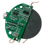 Wireless Charger PCBA
| 5 star | 0% | |
| 4 star | 0% | |
| 3 star | 0% | |
| 2 star | 0% | |
| 1 star | 0% |
Sorry, no reviews match your current selections
Questions & Answers
1. How does the wireless charger PCB work for wireless chargers?
The wireless charger PCB has a transmitter coil that can generate an alternating electromagnetic field when powered. When connected to the device, the magnetic field induces a current in the receiver coil and converts it back into electrical energy to charge the device.
2. Can your wireless charger PCBs handle high currents?
Yes, our wireless charger PCBs can handle moderate to high currents, depending on the application.
3. What frequency range do wireless charger PCBs typically operate at?
Most wireless charger PCBs operate in the range of 110-205 kHz, especially those PCBs that follow Qi standards for inductive charging.
4. What special design features are included in wireless charger PCBs?
Wireless charger PCBs are designed with several key features, such as integrated coils or connectors, resonant capacitors, FOD circuits, a communication module, high-efficiency power conversion components like ICs, and more.
5. Can MOKOPCB provide custom PCB design and prototyping services?
Yes, we totally provide custom and prototype services to offer you the optimal PCB solution. Contact us freely with your specific design requirements.
6. What certifications should a reliable wireless charger PCB manufacturer have?
ISO 9001, ISO 14001, IPC-A-610 certification, and compliance with RoHS environmental standards are required, and you can judge whether PCB manufacturers are reliable through them.

