Via-in-Pad
Via-in-pad technology is very important in supporting the modern high-density PCB design, given increasing compactness, and complexities of electronic devices. The trend toward miniaturization has forced chip manufacturers to develop components with finer pitches like BGAs, QFNs and flip chips, all of which need more advanced routing capabilities. In order to address these problems without compromising signal integrity, PCB designers are combining via-in-pad plated over (VIPPO) structures with traditional design approaches. This integration has a good routability and allows to create reliable and high performance circuit boards.
What Is Via-in-Pad?
Via-in-pad is a PCB design technique where the via is directly put on the surface mount device (SMD) pad, whereas traditional vias are typically located in a non-component zone. This method is typically utilized in high-density designs to save space and simplify routing since signal paths are shortened. In addition, the electrical performance of the circuit boards can also be enhanced through via in pad.
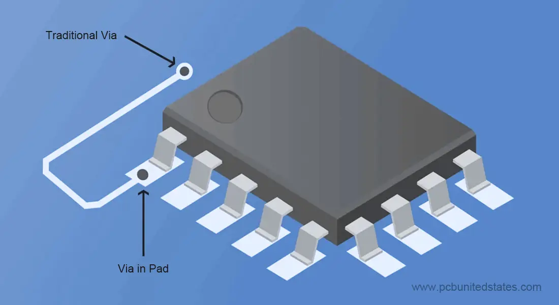
Via in Pad vs. Traditional Vias
The comparison table of via in pad to traditional vias in various aspects follows below:
| Aspect | Traditional Vias | Via-in-Pad |
|---|---|---|
| Location | Non-component areas of PCB | Directly on SMD pads |
| Connection Method | Requires separate traces to connect pads | Direct connection between pad and via |
| Routing Approach | Pass through non-component areas, connect to traces on other side | Enables direct connections to inner/bottom layers |
| Space Usage | Consumes additional PCB space for via placement and trace routing | Maximizes space by eliminating via keepout areas |
| Manufacturing Requirements | Standard through-hole technology, well-established | Requires specialized filling and plating processes |
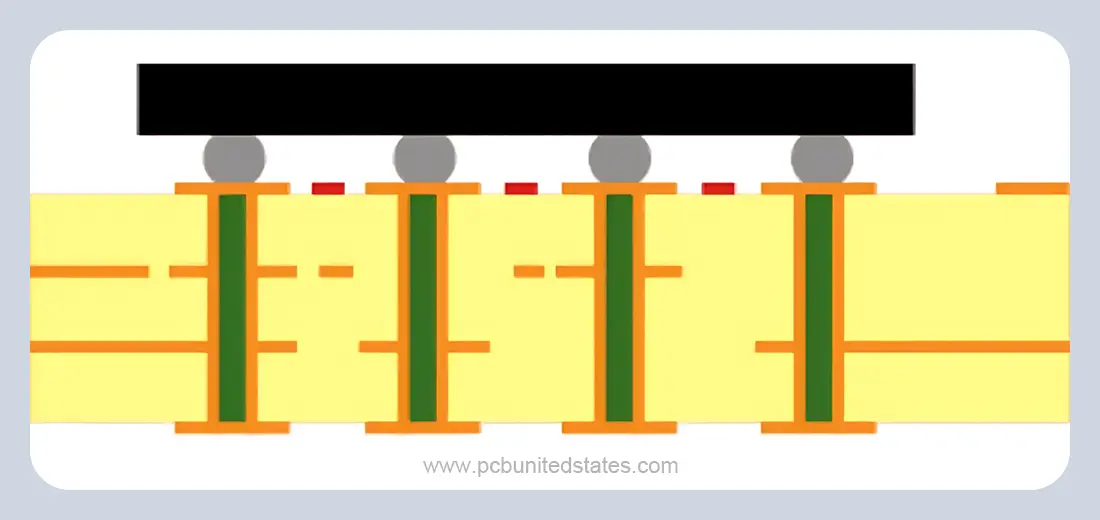
Via-in-Pad Filling Process
Non-conductive epoxy is typically used to fill the vias in via in pad, and once filled, the vias are capped and plated over. This prevents the solder from leaking down into the via during reflow, which can cause unreliable solder joints or even cause shorts. By filling the via entirely, it helps to prevent voids as well as improve plating uniformity.
It should be mentioned that this process is unlike via tenting, in which the solder mask layer simply covers the via without filling it. Tenting could prevent the solder flow to some degree, but does not offer the same structural reliability and soldering quality as filled and capped vias.
Some via-in-pad designs can use conductive material such as copper to fill the via so as to provide a direct electrical connection between the via and pad. This does not require additional trace routing, and the overall size of the PCB is reduced, thereby shortening signal paths and improving signal integrity.
Advantages and Disadvantages of Via in Pad
Via-in-pad has significant benefits at high-density and high-performance PCBs designs, but it comes with a few fabrication difficulties. The following is a list of its advantages and disadvantages:
Advantages
- Maximize the use of PCB space:In this method, viascan be placed directly under the SMD pads so that board surface space is utilized to maximum extent.
- Better thermal performance: Via in pad helps to improve the heat dissipation and keep the temperatures of components within the limited range. This is very critical in high-power PCBs.
- Enhanced PCB Performance: Each via incurs inductance and resistance which slow down current flow. These electrical impedances adversely affect the functionality of the PCB. When using viainpad technology, the power delivery path is reduced, and that significantly improves its performance.
Disadvantages
- Process complexity: Via-and-pad covering process can lead to an uneven surface that requires additional corrective operations.
- Extended manufacturing time: After the drilling, the via-in-pad would have to be filled with epoxy and then plated; this would increase the total production time.
- Increased manufacturing expenses: Via-in-pad structures are complicated and have multiple processing steps, thus relatively costly to produce.
When to Use Via in Pad?
To make optimal PCB-design decisions, you have to grasp when it is necessary to make use of via in pad and when the simple routing approach will apply.
Via-in-Pad Is Required When:
- Tight Pin Spacing: In BGAs whose pin pitch is less than 0.35mm, the space between the pads is too tight to fit vias and traces using standard fanout technique.
- High Pin Density: Components that have a large number of pins would create many fanout traces, which takes lots of routing space. Via in pad design saves precious routing space since there is no need to use extra space around each via.
- Layer Routing Constraints: When layer routing constraints happen on the same layer, via-in-pad serves as a way to connect to inner routing layers or the bottom layer, which has more routing space.
Via-in-Pad Is NOT Required When:
- For BGA components with low pin density and pin pitch greater than 0.35mm, standard fanout routing is possible with vias between the solder pads. There is no need to use via-in-pad.
- The specifications of standard BGA fanout :
- Via diameter: 0.15-0.2mm
- Trace width: 3-4mil
- The width of the annular rings is between 0.3 and 0.4mm.
- Such parameters can be used to do normal routing without having to use via in pad technology.
Guidelines for Via-in-Pad Routing
In order to minimize production difficulties, limit costs, and maintain long-term reliability, there a certain rules of thumb you should observe when employing via in pad in your PCB design, especially in surface-mount devices:
- Place, cap and fill these components according to the manufacturer’s suggestions to ensure compatibility and consistent soldering quality.
- When microvias are used, they should be placed in only one PCB layer, so as to ensure structural integrity as well as ease of fabrication.
- Never leave the non-component side of the via without solder mask, as this would expose them to the environment.
- Do not leave any vias open unless there is no other choice available, because bare copper can oxidize, which makes the PCB less reliable and shortens its lifespan.
- Design pad size according to the via diameter and comply with IPC Class 2 or 3 annular ring requirements, ensuring proper solder joint creation and electrical isolation.
- Fully fill and planarize the vias (epoxy-, or copper-filled) to give a flat surface, which is critical to reliable BGA placement.
- With via-in-pad designs, you can sometimes skip via-plugging under components, since the component itself can stop solder wicking.
Contact Us
Got any questions or inquiries? Fill out the form and we will get back to you soon